
Editor’s Note: This article is excerpted from a presentation titled Novel Surface Finish for 5G-mmWave Frequency PCB Technologies: How to Achieve Optimum Signal Integrity.
0
Introduction
With the increasing demand for high-frequency electronic devices, the shortcomings of traditional surface treatment processes such as electroless nickel immersion gold (ENIG) on printed circuit boards (PCBs) have become increasingly prominent. The fundamental reason is that the presence of the nickel layer leads to increased conductor loss. This article proposes an innovative solution for nickel-free surface treatment—using a nano-scale barrier layer with a gold structure to enhance performance in high-frequency applications. This method aims to address the rapid iteration challenges in the electronics industry while achieving better reliability.
1
The Impact of Nickel and the New Nickel-Free Coating
With the rapid development of mobile phones/devices, the internet, and portable/wearable devices, the amount of wireless network information transmission has also increased significantly. To transmit the data required by current standards, electronic device manufacturers are adopting high-speed, high-frequency electronic signals. The integrity of high-frequency signals is affected by the choice of PCB materials used in manufacturing receiving devices. In PCBs such as those in wearable devices, the combination of high-frequency signals and fine traces may lead to signal loss, affecting performance.
Conductor loss is a major factor affecting the integrity of high-frequency signals, primarily influenced by the coating layer applied to the PCB copper connection pads[1-2]. Generally, ENIG is commonly chosen among applicable coating layers. Due to the presence of nickel, ENIG may lead to increased insertion loss, as shown in Figure 1. The conductivity of nickel is one-third that of copper, resulting in higher conductor loss[3]. Additionally, the nickel-phosphorus (Ni-P) layer has ferromagnetic properties, which can affect circuit performance[4]. Within the frequency range of 0-50 GHz[3-5], the insertion loss of ENIG-coated copper conductors gradually increases compared to bare copper. Figure 1 shows the loss of a GCPW transmission line using an 8 mm thick laminate with a trace width of 0.279 mm and a spacing of 0.165 mm.
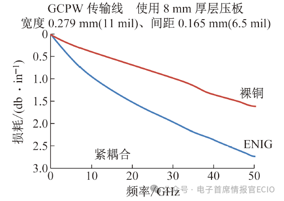
Figure 1: Insertion Loss of High-Frequency Bare Copper Circuits vs. ENIG Copper Circuits
Comparison[3]
As frequency increases, current density concentrates towards the surface coating of the conductor rather than the entire copper cross-section (see Table 1). Therefore, the choice of coating is crucial, affecting insertion loss.
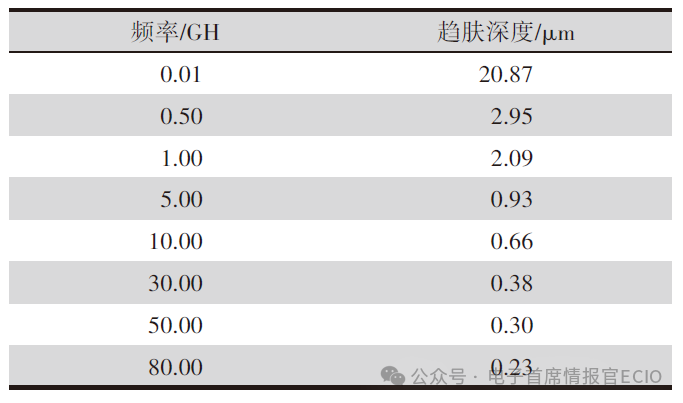
Table 1: Relationship Between Skin Depth and Frequency
Currently, the 5G cellular networks used globally are operating in the high-end millimeter frequency bands. For example, Verizon in the United States is using the 29 GHz band, while AT&T is using the 39 GHz band[6]. Due to the higher data throughput available at higher frequencies, cellular networks between 50-100 GHz have entered the research phase[7], such as automotive radar using the 76-81 GHz band[8]. The signal loss associated with nickel in ENIG coatings has become a signal speed issue for existing cellular networks, and this concern will only intensify as future technologies continue to increase signal speeds. The number of high-frequency PCBs has already accounted for 15% of the entire electronics industry, and this is expected to grow[9].
With the growing demand for high-frequency application PCBs, the requirements for developing new coatings to replace ENIG in this field are as follows:
-
Nickel-free, to eliminate the high insertion loss and ferromagnetic elements associated with ENIG coatings.
-
Gold-coated, to maintain the high reliability and long shelf life currently associated with ENIG.
A coating solution that meets these two requirements can reasonably replace ENIG in high-frequency applications without compromising ENIG’s advantages in low-frequency circuits.
This article discusses a nickel-free surface coating solution for high-frequency applications. In this method, a barrier layer is deposited on bare copper to replace the nickel in ENIG, followed by the deposition of gold on the barrier layer, as shown in Figure 2. This method does not contain nickel, thus it does not affect the insertion loss of high-frequency circuits while still ensuring the reliability of the gold coating.
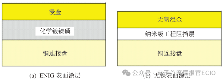
Figure 2: Nickel-Free Surface Coating Replacing ENIG Surface Coating
2
Results of Nickel-Free Coating
2.1 Insertion Loss
The comparison of insertion loss between ENIG coating and nickel-free coating is shown in Figure 3. In the frequency range of 0-100 GHz, the insertion loss of the nickel-free coating is almost identical to that of bare copper. This indicates that the nickel-free coating can be used for high-frequency applications, with almost no increase in insertion loss compared to bare copper. The loss of ENIG at 50 GHz is approximately 2.75 dB/in, while the insertion loss of the nickel-free coating at 50 GHz is about 1.25 dB/in, representing a reduction of over 50% in insertion loss. The difference in insertion loss between the nickel-free coating and bare copper is minimal, making the nickel-free coating solution a good coating for high-frequency applications.
At a frequency of 25 GHz, the comparison of insertion loss between ENIG coating and nickel-free coating is shown in Figure 3. In Figure 3(a), the GCPW transmission line uses an 8 mil thick laminate with a trace width of 0.279 mm and a spacing of 0.165 mm. At 25 GHz, the loss caused by ENIG exceeds 78.74 dB/m. In Figure 3(b), an 18 μm ED copper with a thickness of 0.125 mm is used for the RO3003TM laminate.
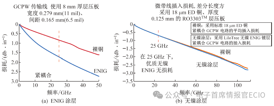
Figure 3: Comparison of Insertion Loss Between ENIG Coating and Nickel-Free Coating (Especially at 25 GHz Frequency)
The figure compares the loss of different treatment methods, including the average insertion loss of bare copper (standard 18 μm ED copper) tightly coupled GCPW circuits and the insertion loss of nickel-free coating (using LitoTree nickel-free ENIG coating) tightly coupled GCPW circuits. At 25 GHz, the high-quality nickel-free ENIG shows no loss.
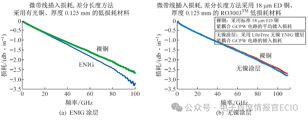
Additionally, electroless palladium immersion gold (EPIG) has shown potential as a nickel-free coating. Its process involves depositing a 0.152-0.203 μm thick layer of electroless palladium on the copper surface, followed by a 0.152-0.203 μm thick immersion gold layer on the palladium layer. EPIG exhibits insertion loss at higher frequencies, while the nickel-free coating shows minimal insertion loss at 100 GHz, as shown in Figure 4. The insertion loss test of the microstrip line with EPIG coating uses bright copper with a thickness of 0.125 mm of low-loss material. The differential length method is used to evaluate the loss performance of different treatment methods; the microstrip line insertion loss test with nickel-free coating uses 18 μm thick ED copper and a thickness of 0.125 mm RO3003TM laminate.
Click to view larger image
Figure 4: Comparison of Insertion Loss Between EPIG and Nickel-Free Coating
The comparison of insertion loss between ENIG, EPIG (EPAG), and nickel-free coatings at different Au (gold) thicknesses is shown in Figure 5. As seen in Figure 5, under 20 GHz conditions, the high-quality nickel-free coating shows no loss, while ENIG causes losses of >2 dB/in. In the figure, C1 represents ENIG (Ni: 5.50 μm, Au: 0.03 μm) coating, C2 represents ENIG (Ni: 5.50 μm, Au: 0.06 μm) coating, C3 represents ENIG (Ni: 5.50 μm, Au: 0.10 μm) coating, C4 represents EPAG (Pd > 0.1 μm Au: 0.10 μm) coating, and C5 represents LitoTree (nickel-free IG) coating.
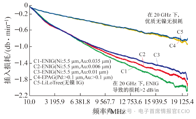
Figure 5: Comparison of Insertion Loss Between ENIG, EPAG, and Nickel-Free Coatings
As shown in Figure 5, compared to other options, the nickel-free coating exhibits excellent performance in terms of minimal insertion loss; additionally, the performance of ENIG is poorer when the Au thickness is smaller. The analysis indicates that more signals pass through the Au layer in thicker Au (ENIG) layers rather than through the electroless nickel (NiP) layer.
2.2 Intermetallic Compounds (IMC) Comparison with Direct Immersion Gold (DIG)
This study aims to compare the intermetallic compound (IMC) status of nickel-free coating samples with a barrier layer against nickel-free coating samples with direct immersion gold (DIG) without a barrier layer.
The test parameters for DIG coatings from the literature[10-11] (see Table 2) use coatings with thicker gold, which only undergo one or two reflow soldering processes. In this study, the nickel-free coating samples underwent six reflow soldering processes. Additionally, under 150°C conditions, thermal storage for 1000 hours was conducted, which is consistent with the parameters of the nickel-free coating samples (see Figure 6).
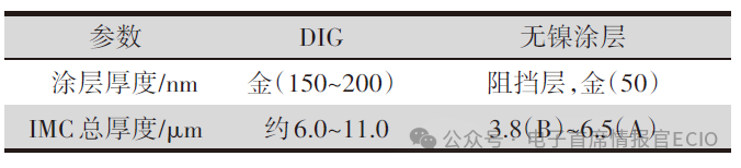
Table 2: IMC of DIG Published in Literature
Comparison with Nickel-Free Coating IMC Data [10-11]
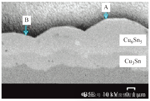
Figure 6: Instances of Nickel-Free Coating IMC After 6 Reflows and 1000 Hours Aging
Despite the stricter sample preparation for nickel-free coating samples, the IMC of nickel-free coatings is consistently thinner than that of DIG coatings, as shown in Table 2. This data is consistent with expectations, as DIG coatings do not have a barrier layer to prevent mutual diffusion between copper and gold, leading to IMC growth. Since the intermetallic compounds of DIG are thicker than those of nickel-free coatings, solder balls on nickel-free coatings should be more secure than those on DIG coatings.
2.3 IMC Comparison with EPIG/EPAG
This study aims to understand the comparison of the barrier layer composition of nickel-free coatings with the barrier layer composition of different surface coatings (such as the 100 nm palladium layer in EPIG/EPAG surface coatings).
The references for EPIG/EPAG coatings in Table 3[12-13] show that during sample preparation, both EPIG and EPAG used a 100 nm palladium layer and a 100 nm gold layer. One sample underwent only 300 hours of thermal storage, while the nickel-free coating sample and another EPAG sample underwent 500 hours of thermal storage. Additionally, compared to the six reflows of the nickel-free coating sample, EPIG/EPAG samples underwent only one reflow.
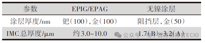
Table 3: IMC of EPIG Published in Literature Compared to Nickel-Free Coating IMC Data
Comparison[12-13]
Despite the stricter preparation of nickel-free coating samples, the results show that the IMC of nickel-free coatings is consistently thinner than that of EPIG/EPAG coatings. This indicates that the barrier layer in nickel-free coatings is better at suppressing IMC growth than the 100 nm palladium layer. Since the IMC of EPIG/EPAG is thicker than that of nickel-free coatings, solder balls on nickel-free coatings should be more secure than those on EPIG/EPAG coatings.
Both DIG without a barrier layer and EPIG/EPAG coatings with a 100 nm palladium barrier layer exhibit IMC growth, while nickel-free coatings with nano-engineered barrier layers suppress IMC growth. The thinner IMC region in solder balls on nickel-free coatings should produce more secure solder joints.
2.4 Solder Joint Strength: Solder Ball Pull Test and Shear Test
The different types of failure modes of solder balls on nickel-free coatings in pull tests and shear tests are shown in Figure 7. After reflow and 1000 hours of aging, the visible failure modes are mode 1 ductile solder ball failure and mode 2 pad lift failure. These two failure modes are related to the solder and laminate rather than defects in the coating of the samples.
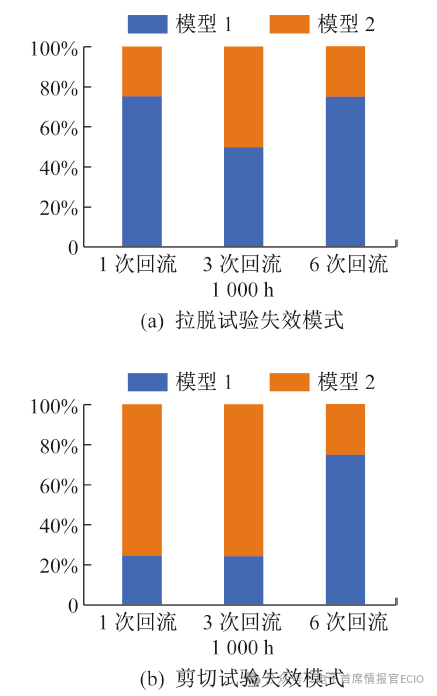
Figure 7: Failure Modes in Pull and Shear Tests of Solder Balls on Nickel-Free Coatings
As seen in Figure 7, neither the solder ball pull nor shear tests showed failures related to the coating, confirming the prediction that the thinner IMC is more stable. Due to the absence of brittle IMC failures, nickel-free coatings produce more robust solder joints compared to ENIG.
3
Conclusion
The new nickel-free coating is a cyanide-free immersion gold deposited on a nano-engineered barrier layer on copper, which is a viable solution for high-frequency high-density interconnector (HDI) applications. Tests on the coating’s intermetallic compound growth, solder ball brittleness failure, and insertion loss show that this new surface coating performs better than currently available nickel-free coatings (such as DIG and EPIG/EPAG), as it has a thinner intermetallic compound layer, no brittle solder joint failures, and extremely low insertion loss (similar to bare copper). Currently, for the reliable final coating layer required in high-frequency HDI PCB applications, nickel-free coatings with nano-engineered barrier layers are a good solution.
References
-
“Effects of Surface Finish on High Frequency Signal Loss Using Various Substrate Materials,” by D. Cullen, IPC APEX EXPO Conference Proceedings, 2001.
-
“Surface Finish Effects on High-Speed Signal Degradation,” by X. Wu, IEEE Transactions on Advanced Packaging, pp. 31, No. 1, 2008.
-
“The Effects of PCB Fabrication on High-Frequency Electrical Performance,” IPC APEX EXPO Conference Proceedings, 2016.
-
“Ambiguous influences affecting insertion loss of microwave printed circuit boards,” by J. Coonrod, IEEE Microwave Magazine, pp. Vol. 13, No. 5, 2012.
-
“Revisit Nickel Characterization Effect on High-Speed Interconnect Performance,” by Y. Tao, in IEEE MTT-S International Conference on Numerical Electromagnetic and Multiphysics Modeling and Optimization (NEMO), 2015
-
“How are 4G and 5G Different?,” by T. Fisher, July 3, 2019.
-
“Propagation Channel Characterization for 28 and 73 GHz Millimeter-Wave 5G Frequency Band,” by T. Abbas, IEEE 15th Student Conference on Research and Development (SCoReD), 2017.
-
“High-Frequency, High-Speed: An Opportunity for China CCLs to Lead,” by Tulip Gu, i-Connect007, July 24, 2017.
-
“The future development trend of PCB and Flexible PCB industry,” J. Ding, Linkedin, June 4, 2018.
-
“Solder joint reliability of Gold Surface Finishes (ENIG, ENEPIG, and DIG) for PWB Assembled with Lead-Free SAC Alloy,” by G. Milad and D. Gudeczka, Uyemura International Corporation.
-
“Evaluation of DIG (Direct Immersion Gold) as a New Surface Finish for Mobile Applications,” by D. Kim, Intel Corporation, 2005.
-
“Characteristics of EPIG Deposits for Fine Line Applications,” by G. Milad and D. Gudeczka, Uyemura International Corporation.
-
“Scaling Cu pillars to 20 um pitch and below: critical role of surface finish and barrier layers,” by T.-C. Huang and M. Tomic, in IEEE 67th Electronic Components and Technology.




This is a collaboration partner of the Chief Electronics Officer (partial)
Order does not indicate priority