“ 12nm process, 2.5GHz frequency, practical training on Cortex-A72 processor backend”
01
Cortex-A72 Processor—Digital Backend Practical Training
This project is a real project practical training, focusing on low-power UPF design, with backend parameters as follows:
Process: 12nm
Frequency:2.5GHz
Resources:2000_0000 instances
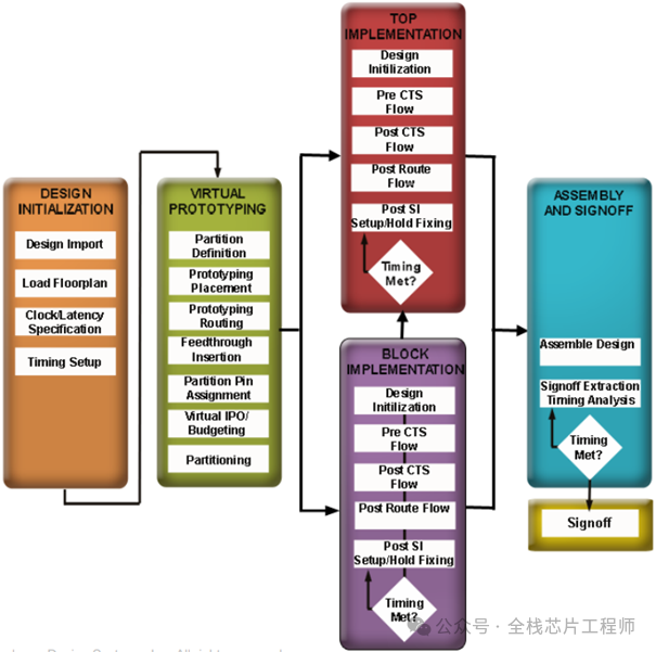
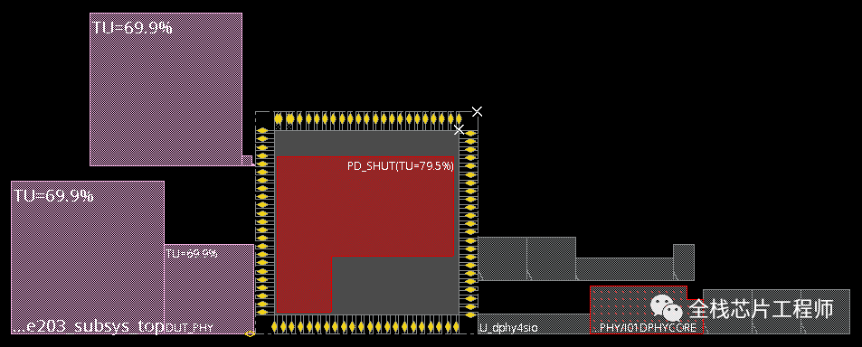
Flow:Partition Flow
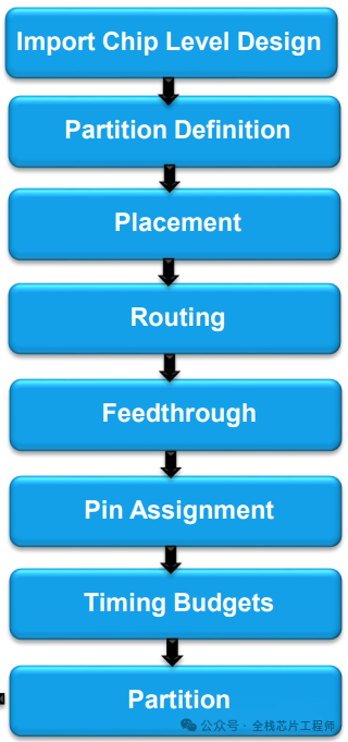
Partition Steps::
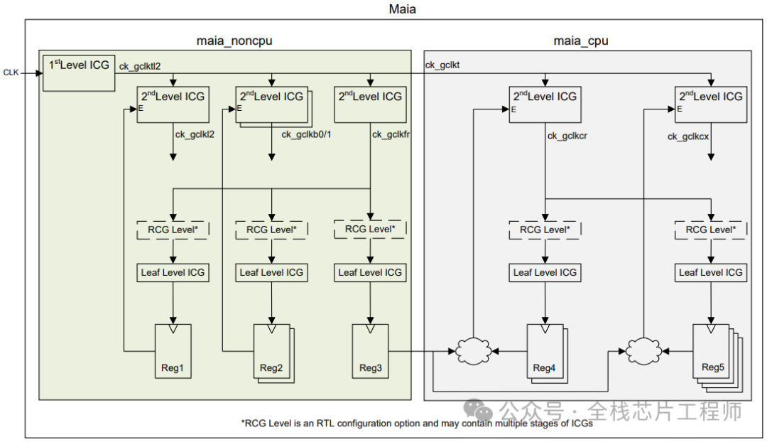
Clock Structure Analysis:
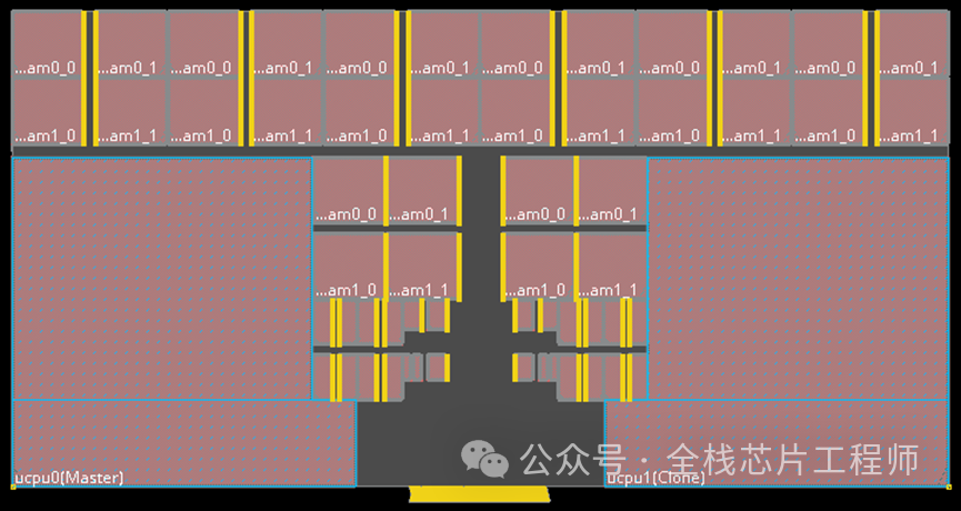
Repetition Structure Analysis:
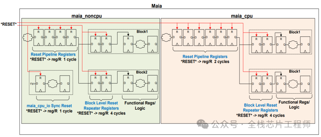
Cortex-A7 Single Core:
Gates=240291 Cells=118421
Cortex-A72 Single Core:
Gates=3125649 Cells=12077666
28nm Cortex-A7 Single Core:
12nm Cortex-A72 Single Core:
Area=486100.9 um^2
02
—
Cortex-A72 Processor—DFT Practical Training
In development, stay tuned.
03
—
Jingxin SoC—Full Chip UPF Backend Practical Training
Jingxin SoC training for full chip UPF low-power design (including DFT design)
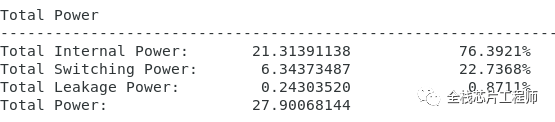
Before low-power design training, power consumption was 27.9mW.
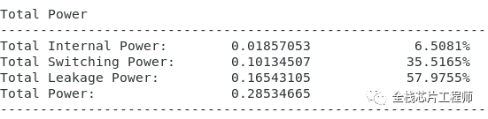
After low-power design, power consumption was 0.285mW, a reduction of 98.9%!
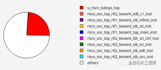
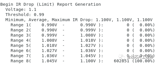
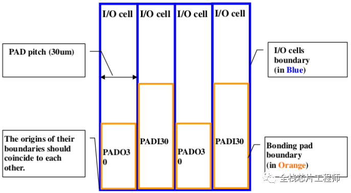
In the 7-day sprint PR training camp, some students asked, with the same floorplan, some students finished quickly while others encountered numerous DRC issues (EDA tools iterating continuously), preventing the tools from completing. What is the specific issue?
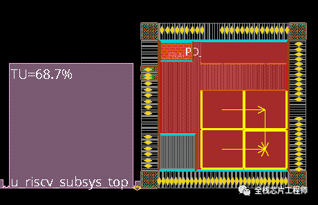
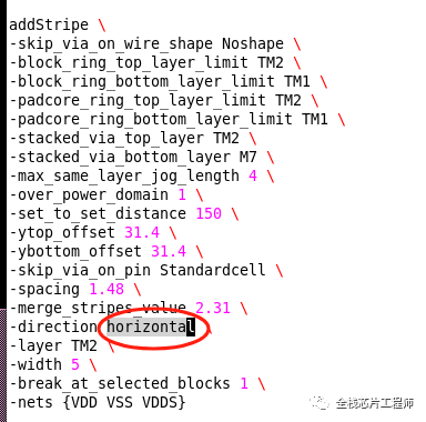
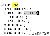
Firstly, I found that the stripe defined TM2 as horizontal, while those familiar with Jingxin technology know that the preference direction for TM2 is VERTICAL.
Checking Jingxin’s LEF library file can also confirm:
How much impact does using the wrong direction have? Everyone should practice the backend flow of Jingxin SoC to gain real knowledge.
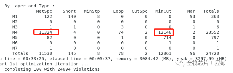
In the 7-day sprint PR training camp, some students asked why PR took a whole day and night (24 hours) to complete routing while still having numerous DRC errors? I have minimized the design scale to speed up PR design; in fact, routing can be completed in 2 hours. Why is it so slow? The reason is the routing of low-power cells. For specific reasons and solutions, please join the Jingxin training camp for discussion.
The errors are mainly concentrated on M4; please think about how to solve them.
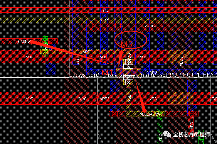
In the 7-day sprint PR training camp, some students asked why the second PG pin (VDDG) of the power switch cell was connected from M1 instead of M2? What issues could arise? How to solve it?
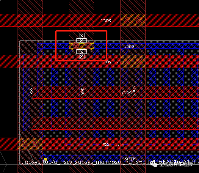
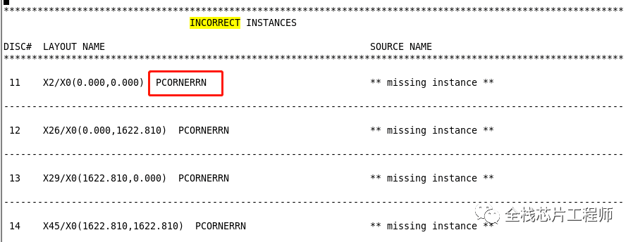
In the 7-day sprint PR training camp, some students asked how to handle the LVS issues encountered by Jingxin SoC training camp students with Corner Pad?
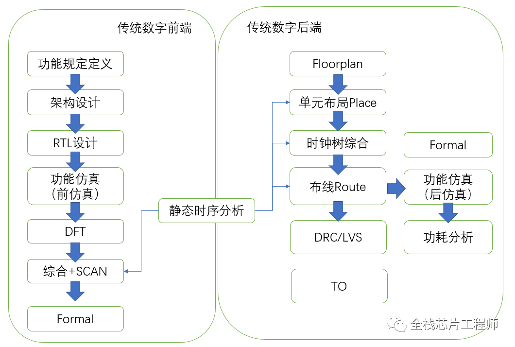
After completing the frontend design simulation and DFT of Jingxin SoC training, we arrive at the backend flow. This tutorial teaches you how to run the digital backend flow with one click.
Generate script command as follows:
tclsh ./SCRIPTS/gen_flow.tcl -m flat all
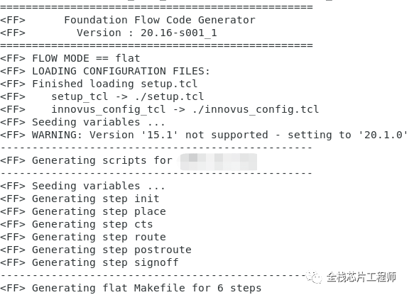
Before generating the flow script, it is necessary to configure setup.tcl and other related parameters. For details, please refer to the unique full-stack chip engineer’s training program provided by Jingxin SoC, guiding you through the entire process from algorithms, frontend, DFT to backend in SoC project design.
Students in the Jingxin SoC training camp ask why Innovus reports an error when reading the completed floorplan def file? First, check the log:

Reading floorplan file – ./data_in/DIGITAL_TOP.def (mem = 1595.0M).
#% Begin Load floorplan data … (date=10/23 22:38:01, mem=1579.3M)
**ERROR: (IMPFP-710): File version unknown is too old.
In the past EDI period, we could load the floorplan by defining fp_file:
set vars(fp_file) “./data_in/DIGITAL_TOP.def”
But now Innovus has upgraded and abandoned the fp_file loading method. Of course, you can use the old version of EDI 9.1 and earlier to add fp_file and then save it as a new version, but this method is clearly unnecessary. As the log suggests, checking the log is an excellent engineering habit.
Input floorplan file is too old and is not supported in EDI 10.1 and newer.
You can use EDI 9.1 and before to read it in, then save again to create new version.
My intuition tells me to check which def version the student saved?
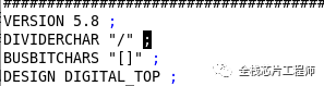
The student’s saving method is as follows:
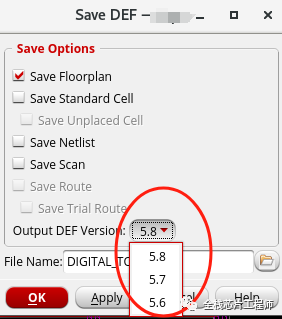
So how to solve it? Please join the Jingxin training camp for practice.
Jingxin SoC uses many asynchronous FIFOs; students interested in asynchronous RTL implementation can extract asynchronous FIFO to observe the layout connections:
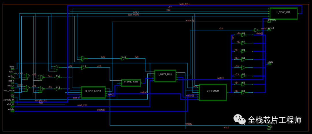
Check the area of all asynchronous FIFO cells;
dbget [dbget top.insts.pstatus unplaced -p].area
Check the names of all asynchronous FIFO cells:
dbget [dbget top.insts.pstatus unplaced -p].name
So how to extract asynchronous paths to observe the layout routing? How to report timing? For more content, please refer to the knowledge community and SoC training camp.