 1. Automotive Chips are the Cornerstone of Software-Defined VehiclesIntelligent, connected, electrified, and shared vehicles are the development trends in the automotive industry in recent years and the future. Cars are gradually moving away from being mere transportation tools, providing users with richer experiences, engagement, and enjoyment. The realization of an outstanding user experience heavily relies on software. Currently, automakers, suppliers, and new players all hope to seize the initiative in this new value chain driven by software.
 This trend and change will bring significant challenges and innovations to automotive E/E architecture and software.
 On the software side: As vehicle functions become increasingly complex, the era of software-defined vehicles sees a rapid increase in the volume of automotive software code, complexity, and safety requirements. According to NXP’s predictions, the amount of code in vehicles is expected to grow exponentially from 2015 to 2025, with an average annual compound growth rate of about 21%.
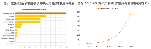 On the architecture side
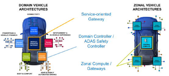
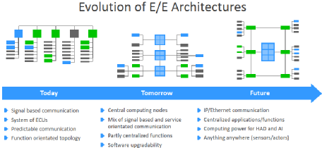 The automotive E/E architecture has traditionally followed a “one function, one box” distributed architecture model. Under this form of automotive electronic and electrical architecture, adding a function requires adding a corresponding controller, further increasing system complexity. Currently, OEMs are gradually moving towards domain control and zone control to integrate software, simplify vehicle wiring, and reduce costs.
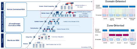 The ultimate goal of E/E architecture is a central computing architecture, composed of heterogeneous multi-core processors, such as ARM Cortex-A architecture, ARM Cortex-M architecture, GPUs, etc. All sensors are intelligent sensors with built-in processing capabilities, and the interaction and control between the central computer and sensors are established through a gateway.
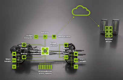 As the saying goes: A good horse deserves a good saddle. Although the vehicle functions based on software are becoming increasingly rich, how can we ensure that the corresponding software operates safely, efficiently, and reliably? Undoubtedly, this must rely on increasingly powerful hardware, and the core of hardware is automotive chips.
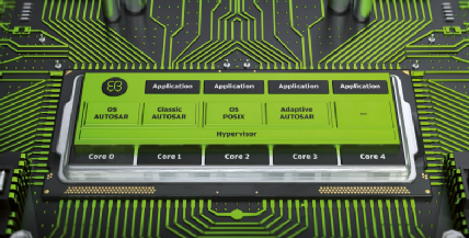 2. NXP Domain Control Chip – S32G
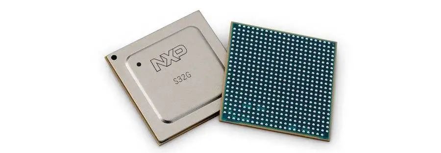
 In the current trend of intelligence and connectivity, major chip suppliers have corresponding product support for domain control and connectivity applications. This article will focus on the NXP domain control chip – the S32G series, which is currently receiving significant attention in the industry.1. NXP S32 SeriesNXP launched the S32 series product portfolio in 2017, covering various application scenarios in vehicles, including body, radar, gateway, chassis power, etc., providing rich product support to OEMs and Tier 1 suppliers.
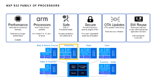 All products in the S32 series share multiple IP cores, allowing software to be shared among different ECUs, such as domain controllers, zonal controllers, and nodes, including basic BSP and related development design results for information security and functional safety.In the current hot background of domain control, as one of the S32 family products currently promoted by NXP, S32G mainly addresses the following target applications:
- Central Gateway: Requires acceleration of deterministic network communication and other processing task loads, and needs to provide embedded security for emerging wireless services.
- Service Gateway: Requires high-performance application processing and provides isolation functions for rapid deployment of new security services.
- Domain Controller: Requires high-performance real-time and application processing to support ECU integration, network protocol conversion, and local control.
- Security Co-Processor: Requires ASIL D functional safety processing and network connectivity and PCI Express® to share data with other components and central large-capacity storage.
- Central Vehicle Control Unit: Under the new electronic and electrical architecture trend, the service gateway integrates more and more functions (e.g., VCU, BCM, etc.).
 Typically, the basic system block diagram of a service gateway or central vehicle control unit based on S32G is as follows, with peripheral circuits requiring dedicated PMIC chip VR5510, CAN and Ethernet transceiver chips, and necessary storage chips.
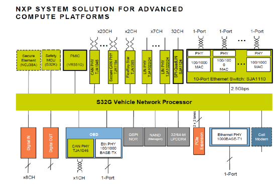 The S32G processor adopts mature and reliable automotive domain-specific technology design and manufacturing, equipped with an embedded hardware security engine (HSE) to meet the high performance, security, safety, and reliability requirements sought by developers.The S32G automotive network processor combines ASIL D level safety, high-performance real-time and application processing, and network acceleration features, with the following main characteristics:
 The S32G is currently mainly the G2 family product, which also provides different product support based on different cost requirements and application scenarios under the G2 family product series.
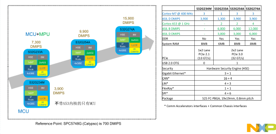
 3. Main Features and Applications of S32G2 Products1. Multi-core Heterogeneity Meets Complex Software Function RequirementsCurrently, as the software functions of vehicles become increasingly complex, coupled with the need for OEMs to integrate the functions of multiple controllers into one controller, multi-core support is increasingly required.
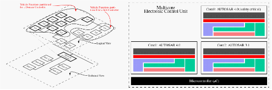 Several factors contribute to the demand for multi-core:Parallel computing requirements: For example, the output calculation of certain functions requires multiple input elements to be executed within the same time slice and input into the function module simultaneously.
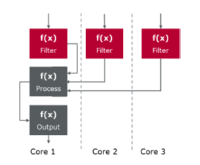 Serial computing requirements for multiple tasks within the same time slice: For example, multiple functions need to be executed serially within the same time frame.
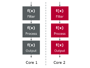 System responsiveness requirements: For example, for those interrupt handling that require particularly high timing, they need to run on a separate core, while periodic tasks are run on another core, thereby improving the overall system responsiveness.
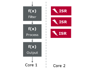 Additionally, within the same controller, we may deploy embedded applications with high real-time requirements, such as control in the Powertrain domain, and also deploy applications with lower real-time requirements, such as vehicle-machine interaction. These software may rely on different operating environments, which could be RTOS, Linux, or QNX. In this case, in addition to the demand for multi-core, heterogeneous core support is also needed to run software that depends on different operating systems.
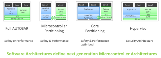 Meanwhile, S32G2 supports up to four Arm® Cortex®-A53 cores with Arm Neon™ technology, with optional lock-step functionality for handling high-computational applications and services. It also has three fully lock-step Arm Cortex-M7 cores for handling real-time applications.
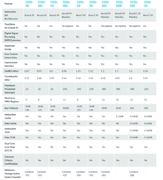
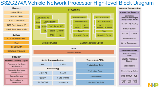 We know that the ARM Cortex core series provides a wide range of scalable performance options, allowing designers to choose the most suitable core for their applications rather than adopting a one-size-fits-all solution. The Cortex series is mainly divided into three categories:
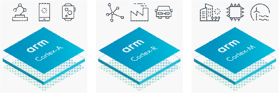 Cortex-A: Application processor cores for performance-intensive systems, similar to CPUs, capable of running Linux, QNX systems, etc.Cortex-R: High-performance cores for real-time applications.Cortex-M: Microcontroller cores for various embedded applications.Therefore, in summary, ARM Cortex-A is widely deployed in applications requiring Linux or other complex operating systems, while Cortex-R and Cortex-M are aimed at real-time embedded applications.
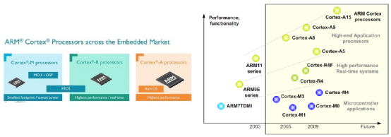 The S32G MCU uses three 400MHz Arm Cortex-M7 cores, with M7’s primary mission being high performance, achieving unprecedented levels while maintaining the series’ consistent ultra-small area and ultra-low power consumption. Architecturally, M7 features a six-stage, in-order, dual-issue superscalar pipeline, with single-precision and double-precision floating-point units, instruction and data caches, branch prediction, SIMD support, and tightly coupled memory (TCM). Instruction and data caches, branch prediction, and TCM are features not previously available in the M series. MCUs often do not consider caching, sometimes even using flash memory as the only memory interface. By incorporating high-performance instruction and data caches (up to 64KB), M7 begins to align with typical high-performance processor designs. TCM, previously only found in A and R series, can be used to extend M7’s effective cache, with a maximum capacity of 16MB, which is part of the MCU’s physical memory mapping.
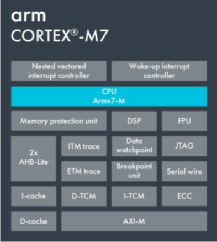 Although the real-time processing core does not adopt Cortex-R, under the same testing environment, the actual measured performance of the S32G’s M7 core (400MHz, 1300 DMIPS) running in SRAM is about 3 to 5 times that of the R5F core (1GHz, 2000 DMIPS) running in DDR.Additionally, the NXP S32G series uses four 1 GHz Cortex-A53 cores. Since the M and A series often coexist and collaborate, this combination achieves a dual advantage, enabling complex software function development based on this chip. For example, Arm Cortex-M7 can serve as an MCU for higher real-time control, such as Classic Autosar applications in the power domain, while Cortex-A53, due to its high frequency and processing capability, is mainly used for running algorithms, such as running infotainment or ADAS domain applications based on QNX’s Adaptive Autosar.The S32G SoC system-on-chip provides an XRDC hardware resource isolation mechanism, ensuring that real-time applications on the M7 core and performance applications on the A53 core can effectively cooperate while being completely hardware-isolated, ensuring high reliability for the entire system.
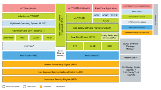 As a heterogeneous multi-core processor, S32G not only uses high-performance main cores but also has many low-performance small cores in various modules. The A core, M core, LLCE, PFE, and HSE modules of S32G all have built-in processors, meaning they can communicate and cooperate with each other to complete various functions, achieving distributed functionality. For example, LLCE has four 200MHz Cortex M0+ cores, similar to traditional CAN gateway MCUs.
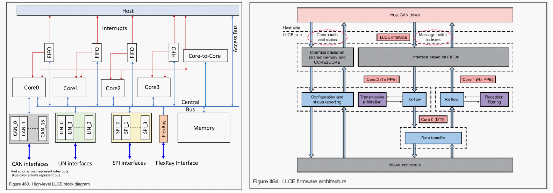 Additionally, the S32G2 Arm® Cortex®-A53 cores come with optional lock-step functionality for handling high-computational applications and services. It also has three fully lock-step Arm Cortex-M7 cores for handling real-time applications. This ensures that some functional safety requirements are met, achieving high diagnostic coverage.
 2. Communication Acceleration Module Supports SOA Gateway ApplicationsWith the trends of automotive intelligence, connectivity, and sharing, end users’ expectations for vehicle functions are also quietly changing. While achieving high-level autonomous driving/assisted driving functions, vehicles are also increasingly inclined to enhance user experience, such as enabling rapid function updates and upgrades, and providing personalized, humanized, and differentiated functions and services. Service-Oriented Architecture (SOA) is providing a good solution for future vehicle software services.
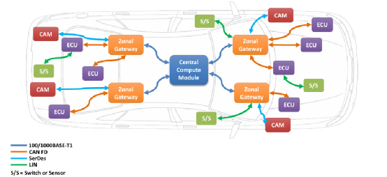 Signal-based communication only supports send and receive modes, with simple data types and poor scalability, suitable for applications with limited data interaction. However, with advanced application scenarios such as autonomous driving, a large amount of dynamic data interaction must adopt service-oriented communication methods to improve communication efficiency and reduce load. In this mode, the receiver acts as a client, simply needing to find and subscribe to services to wait for information, while the sender, as a service provider, only needs to provide services and information to subscribers. Since SOA-based communication supports request/response modes, it is highly scalable and supports the transmission of complex data. SOA applications must be based on Ethernet, and in terms of communication, S32G has rich communication interfaces, including 20 CAN interfaces, 4 Gigabit Ethernet interfaces, and 2 PCIe 3.0 interfaces, providing flexibility for various application scenarios such as gateways or domain control.
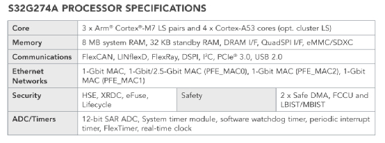 Using S32G with NXP-related Switch and Transceiver products can greatly enhance scalability:
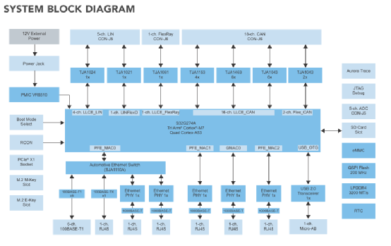 In gateway applications, the data throughput is very high, and network acceleration is one of the key features of S32G. Without it, processing Gigabit Ethernet at full load would consume 90% of the ARM core’s processing capability. With the accelerator enabled, this performance drop is reduced to about 0.2% of usable performance, allowing the CPU to freely handle a series of other tasks. This is mainly due to NXP’s Low Latency Communication Engine (LLCE) and Packet Forwarding Engine (PFE).2.1 Low Latency Communication Engine (LLCE)The LLCE of S32G is primarily responsible for communication with CAN, LIN, and FlexRay. LLCE offloads the main core’s load during checksum and authentication frame processes and can handle frame encryption and decryption based on the on-chip hardware security module (HSE). LLCE aims to provide:• Low-latency processing for communication interfaces• Offloading host core load for all interface-related tasks• Security-related tasks can directly access and transmit data to the HSE module
 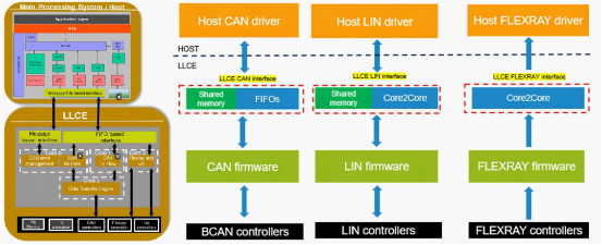 LLCE is a fully programmable engine, and its firmware supports:1. Offloading the main CPU load for all communication interface-related tasks, such as reducing interrupt load on the host core and advanced software filtering.2. Providing flexible control and data interfaces to the host core.3. Providing hardware acceleration for filtering and determining message priority, ensuring low-latency requirements for gateway forwarding applications.The firmware is integrated into the AUTOSAR MCAL communication stack, and NXP provides drivers for CAN_LLCE, LIN_LLCE, and FR_LLCE. The AUTOSAR drivers for LLCE run in parallel with standard communication CAN/LIN/FR drivers. NXP LLCE firmware supports user-created high-level extensions, such as:• Using HSE services for CAN frame authentication• CAN to CAN routing• CAN to Ethernet and Ethernet to CAN routingLLCE handles the following communication interfaces:• 16 CAN interfaces, supporting CAN2.0 and CAN FD (Flexible Data Rate) (5 Mbps)• 4 LIN interfaces, each capable of reaching 20 Kbps• 1 FlexRay interface (20 Mbps)2.2 Packet Forwarding Engine (PFE)PFE significantly reduces the host core’s processing load for Ethernet packets, achieving higher performance and lower power consumption compared to pure software processing methods. PFE has a packet forwarding speed of 2 Gbit/s and imposes almost no load on the host core.
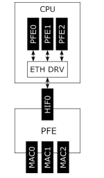 PFE is a firmware-based module. Firmware needs to be loaded before using PFE. The PFE core starts during the host core initialization. After initialization, PFE enters normal mode and is ready to operate fully. PFE is based on a programmable packet processing engine (PE). It implements a fast path and slow path architecture. It can completely offload the host core’s fast path data packets. Slow path data packets (e.g., control data packets) can be processed on the host core. Additionally, PFE’s classification module categorizes and executes header modification tasks, such as Network Address Translation (NAT). NXP provides host interface drivers for PFE.
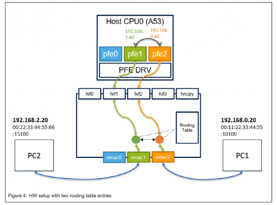 2.3 SummaryThus, S32G uses accelerators to complete CAN and Ethernet routing communication, greatly freeing up the computational power of the M and A cores. Through the cooperation of the accelerators, CAN-to-CAN, CAN-to-Eth, Eth-to-CAN, and Eth-to-Eth routing and forwarding functions can be completed. As communication bandwidth and routes increase, the accelerators can take on more processing tasks without affecting the execution of application software on the A and M cores. After using the accelerators, the computational power required for the gateway, based on actual automotive project experience, is about 0.5 of an M7 core, or 650 DMIPS.3. HSE Supports Information and Communication SecuritySecurity is an eternal topic in every field, and the automotive sector is no exception. In recent years, automotive security has received increasing attention from users and developers. Before the introduction of intelligent connectivity and autonomous driving functions into the automotive field, functional safety was always a top priority. Therefore, functional safety methods and processes are also key parts of automotive industry standards and development. Today, with the emergence of various intelligent connected and autonomous vehicles, features such as vehicle connectivity, vehicle maintenance, and traffic safety information sharing have become increasingly common, while also increasing the likelihood of different motivations for hackers to attack vehicles, thus bringing new risks to automotive network security.Developers focus on and consider the reliability and security of the entire vehicle E/E architecture, hardware, and software, such as hardware EMC and random failures, software functional design, and communication security both inside and outside the controller. Each security element is an important component of the system’s objectives to ensure the reliability and safety of the entire vehicle, thereby protecting user safety.The NXP S32G provides a Hardware Security Engine (HSE) for secure boot and acceleration of security services. HSE, as a security subsystem, is designed to run applications with strict confidentiality or authenticity requirements, featuring functions such as key management, memory checks, encryption and decryption, and random number services:
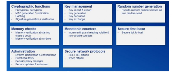 HSE firmware can meet a wide range of automotive security requirements and use cases (AUTOSAR® SecOC, SSL/TLS, IPsec, etc.).
 These services are accessed through flexible and configurable communication interfaces, allowing synchronous and asynchronous requests. These general security APIs allow users to integrate the HSE subsystem into different security stacks.
 4. Complete Chip-Level ASIL-D Functional SafetyAs the in-vehicle central gateway evolves towards central vehicle control (HPC or CCU), more and more functions will be integrated, such as VCU and BMS, which are high functional safety modules, placing higher demands on processors. Additionally, in ADAS/AD applications, traditional independent MCUs used to achieve “safety island” functions are limited by relatively low computing power. The S32G heterogeneous processor provides high-performance processing capabilities while also offering chip-level high-grade functional safety, meeting the application scenarios mentioned above.4.1 S32G Functional Safety FeaturesUnlike the “safety island” approach provided by other SOC products in the industry, S32G offers functional safety implementation at the entire SOC level, designed modularly in a SEooC manner, with M7_0 as the safety master core.The hardware resources include three pairs of lock-step M7 cores, configurable lock-step A53 cores, and basic FCCU, BIST, WDG, clock comparators, as well as additional resources such as ASIL-D buses, XRDC access protection, memory partitioning and protection, lock-step interrupt controllers, lock-step DMA with ECC, error injection management, and reset production management, among other safety modules.4.2 Functional Safety Software Framework (SAF)To facilitate the development of functional safety application software, NXP has developed a functional safety software framework (Safety Software Framework, SAF) for S32G, which allows for code generation through configuration software, making it easy to integrate into AUTOSAR or non-AUTOSAR applications.SAF includes multiple functional modules, including basic drivers (Safety Peripheral Drivers, SPD), as well as more middleware modules such as Safety Boot, Mode Selector, Error Management, Square Check, etc., facilitating rapid development of functional safety application software.
 4.3 Designing ASIL-D SystemsNXP also provides ASIL-D power chips VR5510 to work with S32G, achieving board-level ASIL-D safety objectives.
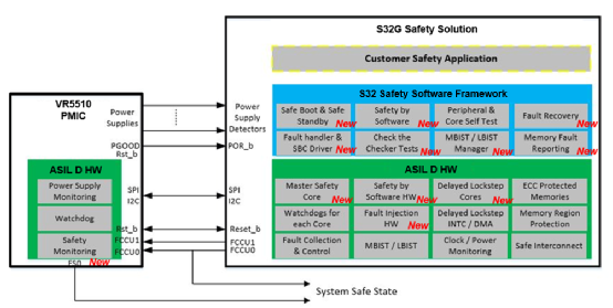 5. Advantages of On-Chip SRAMThe S32G2 features 8MB of on-chip SRAM, connected in a 64-byte interleaved manner. At 400MHz x 128bit, with pipelining capabilities, it achieves maximum throughput. The S32G3 provides up to 20MB of SRAM, further enhancing the integration of real-time core multi-domain fusion.5.1 SRAM Enhances PerformanceHigh-performance computing chips tend to increase on-chip high-speed SRAM to improve execution efficiency. For example, Tesla’s autonomous driving FSD chip has 32MB of SRAM, and Google’s TPU has 24MB of SRAM. Thanks to the on-chip 8MB SRAM, the performance of the S32G2’s real-time core M7 has also been greatly enhanced.In actual tests comparing the performance of the 400MHz M7 core and the 1GHz R5F core, the CoreMark values were 1650/M7 vs. 2020/R5F. In real operating environments, since M7 runs in on-chip SRAM while R5F runs in DDR, the time taken for M7 to run various test cases is significantly shorter than that of R5F, demonstrating the performance improvement brought by on-chip SRAM in practical applications.
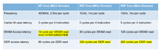 5.2 SRAM Enables Fast Startup and Wake-UpIn traditional gateway applications and the new generation of central vehicle control applications, fast startup/fast wake-up for CAN and Ethernet is an essential function. Different OEMs may have varying requirements, but it is generally required that CAN wake-up occurs within 100ms, meaning the processor must quickly wake up to execute software and route received CAN messages to other ECUs. Nowadays, Ethernet wake-up has similar requirements, as regional controllers (ZCU or VIU) will need to connect to the central vehicle control CCU via real-time Ethernet, requiring short time to send Ethernet data to the CCU and execute corresponding actions. Typically, several necessary conditions for achieving quick wake-up after sleep are as follows:a. A fast interrupt response MCU core is required.b. Real-time code or real-time operating systems, such as AUTOSAR CP, need to be run.c. There must be physical space for immediately executable code after waking up, such as SRAM or Flash.In the past, conventional MCUs could execute code in on-chip Flash Memory, thus meeting the time requirements for wake-up. However, some SOCs require code execution in DDR Memory after waking up, which usually has a longer setup time due to the need for training parameters, thus failing to meet wake-up requirements. (If DDR is not powered off during sleep and remains in self-refresh mode, it may significantly shorten the lifespan of the chips).The S32G2’s built-in 8MB SRAM can run all AUTOSAR CP software in SRAM (S32G3 provides 20MB SRAM), allowing hardware initialization time to be controlled to around 32 milliseconds before jumping to the user’s bootloader code, ultimately achieving fast wake-up functionality.
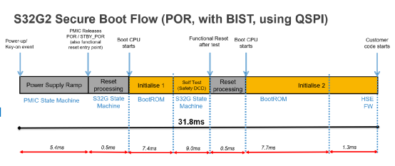 6. Achieving Compatible Design with S32G2/G3In December 2021, NXP released four S32G3 series devices, further expanding the S32G automotive network processor series. Compared to the original S32G2 series, the newly launched S32G3 products offer software and pin compatibility, facilitating platform design, and the S32G3’s computing power, on-chip SRAM, and network bandwidth have been significantly enhanced, allowing for more functions to be integrated into the central vehicle control unit and further supporting intelligent software-defined vehicles.
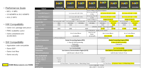 4. ConclusionPerformance: The S32G processor provides MCU and MPU processors that meet ASIL D requirements, with specific application network hardware acceleration to support real-time requirements in complex environments;Information Security: The S32G includes high-performance hardware security acceleration and PKI support for trusted key management;Functional Safety: The S32G provides processors that meet ASIL D requirements, including ARM Cortex-M7 microcontrollers that support synchronous mode (lock-step) and multiple ARM Cortex-A53 application processing cores with lock-step clusters functionality.The S32G, as the latest product in the NXP S32 series, can assist the automotive industry in transitioning to high-performance, domain-based vehicle architectures while reducing software complexity and enhancing information and functional safety.
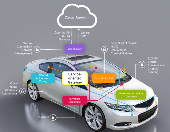 END
END