The security industry is an important sector driven by the safety needs of modern society. With continuous technological advancements, video surveillance technology has evolved from “seeing” to “seeing far,” “seeing clearly,” and finally to “understanding,” pushing the industry from analog surveillance to digital surveillance, network high-definition surveillance, and ultimately into the era of intelligent surveillance. Each leap in technology is inseparable from the innovation of upstream core technologies.
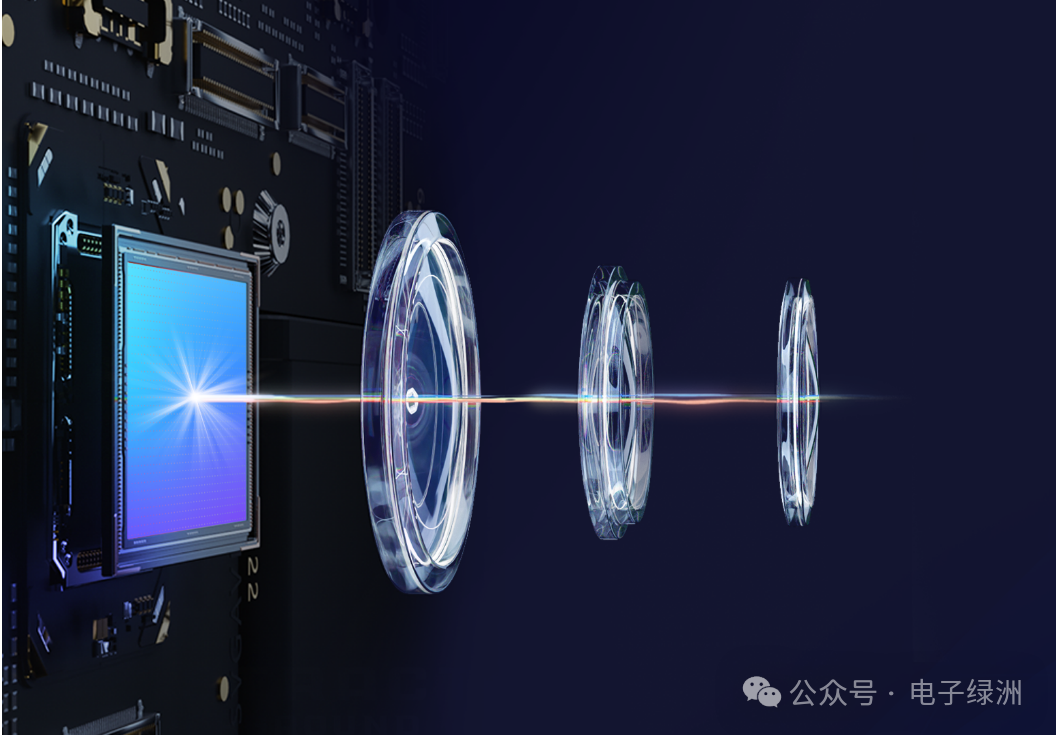
In security monitoring systems, image sensors serve as core components, responsible for converting optical signals into electrical signals, generating high-quality digital images or videos, and providing visual monitoring data for the system. The performance of these sensors directly affects the clarity, sensitivity, and intelligence level of the monitoring system, making them one of the core driving forces behind industry development.
1. Introduction
SmartSens Technology Co., Ltd. (stock abbreviation: SmartSens, stock code: 688213) is a high-tech enterprise engaged in the research, design, and sales of CMOS image sensor chip products, headquartered in the Minhang District of Shanghai, China, with R&D centers in multiple cities and countries. Since its establishment, SmartSens has focused on the innovation and research of high-end imaging technology, gaining recognition and favor from numerous customers due to its performance advantages. As a company dedicated to providing CMOS image sensor products that cover multiple application scenarios and full performance, its products have met the full performance requirements across various application fields, including security monitoring, machine vision, intelligent automotive electronics, and smartphones. SmartSens adheres to the vision of “using cutting-edge intelligent imaging technology to help people better see and understand the world,” with customer needs as the core driving force, continuously promoting the upgrade of cutting-edge imaging technology, expanding product application fields, and working with partners to advance the deep development of future intelligent imaging technology.
2. SC4336P Parameters
Resolution: 4 million
Pixel Array: 2568H x 1448V (16:9)
Pixel Size: 2.0um x 2.0um
Maximum Image Transfer Rate: 2560H x 1440V @30fps 10bit
Optical Size: 1/3″
Output Interface: 8/10-bit 1/2 Lane MIPI
Output Format: RAW RGB
CRA: 15°
Sensitivity: 2813 mV/lux.s
Dynamic Range: 76 dB
Signal-to-Noise Ratio: 37.3 dB
Operating Temperature Range: -30°C~+85°C
Optimal Operating Temperature: -20°C~+60°C
Power Supply: Analog voltage 2.8V, IO voltage 1.8V, core voltage supplied by built-in LDO
Package Size: 35-pin CSP, 5.75mm x 3.872mm
ESD Level: HBM Classification 3A, CDM Classification C3
3. Design References and Considerations
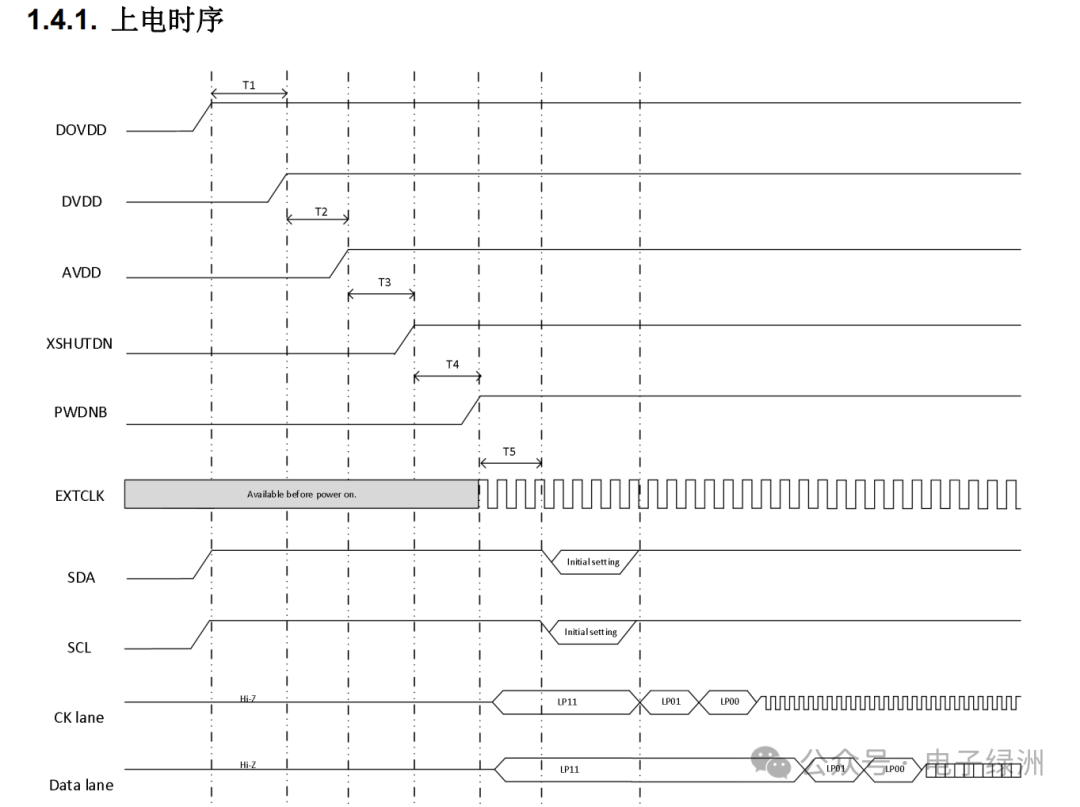
1. Power-Up Timing
1) T1≥0ms, T2≥0ms, T3≥0ms, T4≥0ms, T5≥4ms
2) If DVDD is supplied internally, the power-up timing for DVDD does not need to be considered.
3) If PWDNB and XSHUTDN are not used, pull them up to DOVDD, and there is no need to consider the power-up timing for PWDNB and XSHUTDN.
4) It is recommended that XSHUTDN be controlled by GPIO for hardware reset functionality.
Hardware Design Considerations:
A. Voltage power-up timing: DOVDD 1.8V, DVDD 1.2V, AVDD 2.8V.
B. External DVDD voltage is not required.
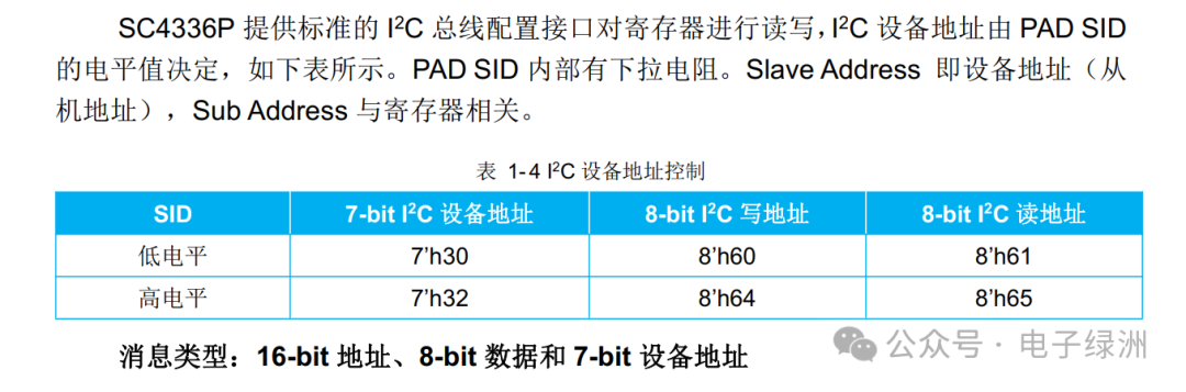
2. I2C Address
The SID pin is a configuration pin; low level is one I2C address, high level is another I2C address. The SID pin must not be left floating.
Hardware Design Considerations:
A. The I2C write address is the I2C device address shifted left by one bit, and the I2C read address is the I2C write address plus one.
B. In typical binocular designs, a single I2C bus is shared, and the SID of the two sensors should be one pulled low and one pulled high.
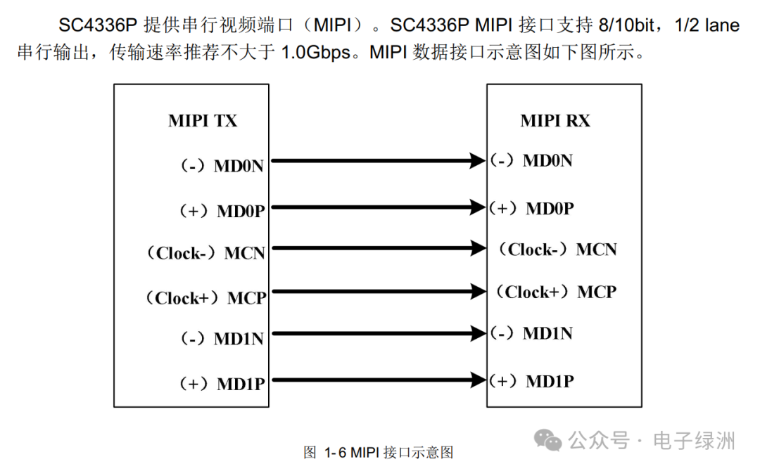
3. MIPI Interface
Supports 1/2 lane data transmission.
Each pixel supports 8/10bit.
Hardware Design Considerations:
A. The differential pair internal line length requirement is 10mil, and the differential pair spacing requirement is 100mil.
B. Avoid placing resistors in series or capacitors in parallel with the differential pairs. In high-speed mode, the typical differential voltage is 200mV.
C. During layout, the three pairs of differential lines should have complete reference ground and should not be split. Avoid vias; if vias are necessary, ensure there are return ground vias.
4. AEC/AGC
The SC4336P does not have AEC/AGC functionality; it needs to be implemented through the backend platform. This means that the backend platform (such as ISP or main control chip) analyzes the brightness and contrast information of the image to determine whether adjustments are needed, and then controls the sensor’s AEC/AGC via I2C.
Hardware Design Considerations:
A. During long-term reliability testing, the software can set the AGC gain to maximum, making it easier to identify hardware issues.
For example, large ripple in the analog voltage of 2.8V can cause stripes; excessive temperature can lead to severe thermal noise.
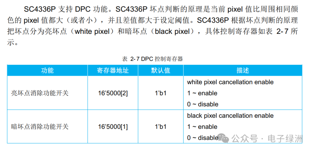
5. DPC Function
DPC: Defect Pixel Correction.The principle of defect judgment for the SC4336P is that the current pixel value is either greater than (or less than) the surrounding pixels of the same color, and the difference exceeds the set threshold.
Hardware Design Considerations:
A. When introducing a new sensor, it is essential to strictly control the number of defective pixels, for example, 30 (Light mode), 30 (Dark mode).
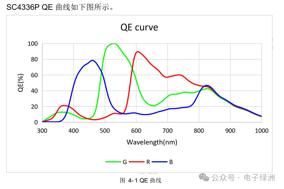
6. QE Curve
Quantum Efficiency (QE) curve describes the response capability of image sensors (such as CMOS or CCD sensors) to photons at different wavelengths. It indicates the sensor’s ability to convert incident photons into electrons, typically expressed as a percentage or the number of electrons generated per photon (e-/photon).
Hardware Design Considerations:
A. Conduct actual tests of images under low and high illumination.
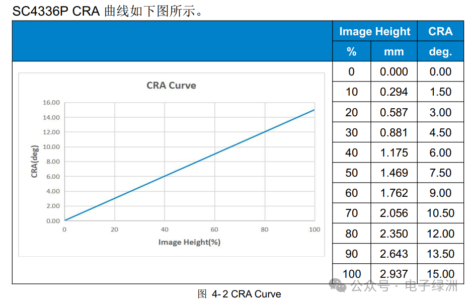
7. Chief Ray Angle (CRA)
The CRA of the SC4336P is a maximum of 15°.
Hardware Design Considerations:
1. The CRA of the lens must match the CRA of the sensor; otherwise, the image will exhibit uneven illumination and dark corners.
8. Packaging
SC4336P Package: 35-pin CSP
Hardware Design Considerations:
A. The Array Center is the optical center and should be aligned with the center of the lens.
B. The pins of SC3336P/SC4336P/SC401AI/SC5336P are Pin to Pin. (However, the DVDD voltage may be supplied internally or externally.)
The physical dimensions of different sensors also vary; when designing restricted areas, consider a margin of 2mm.
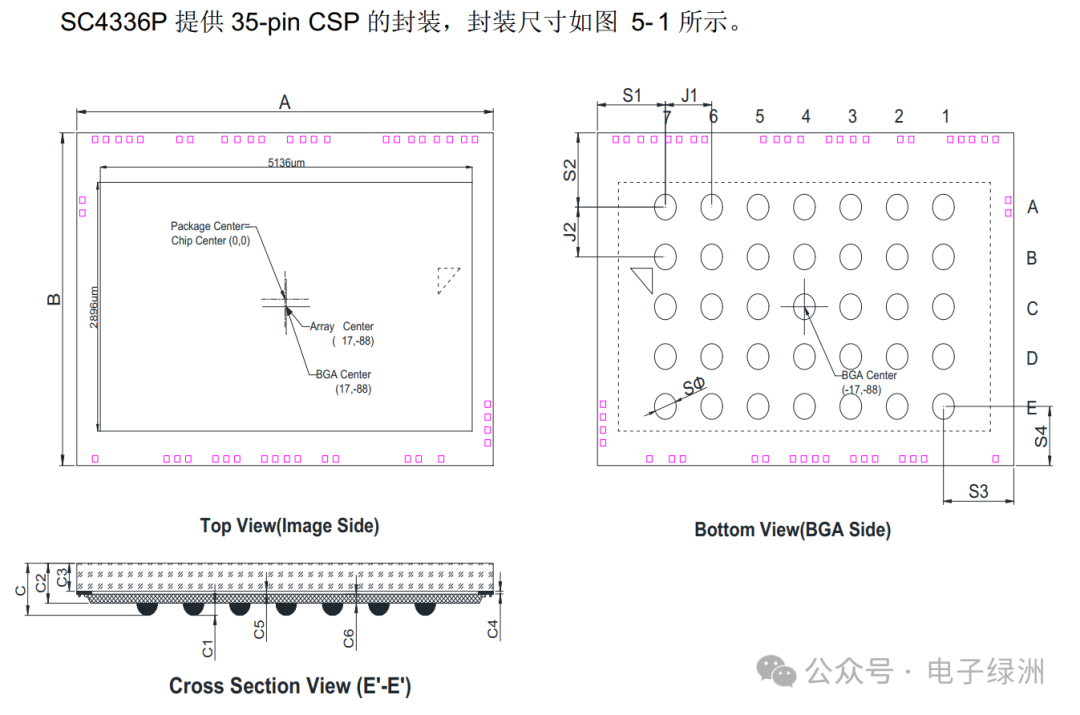
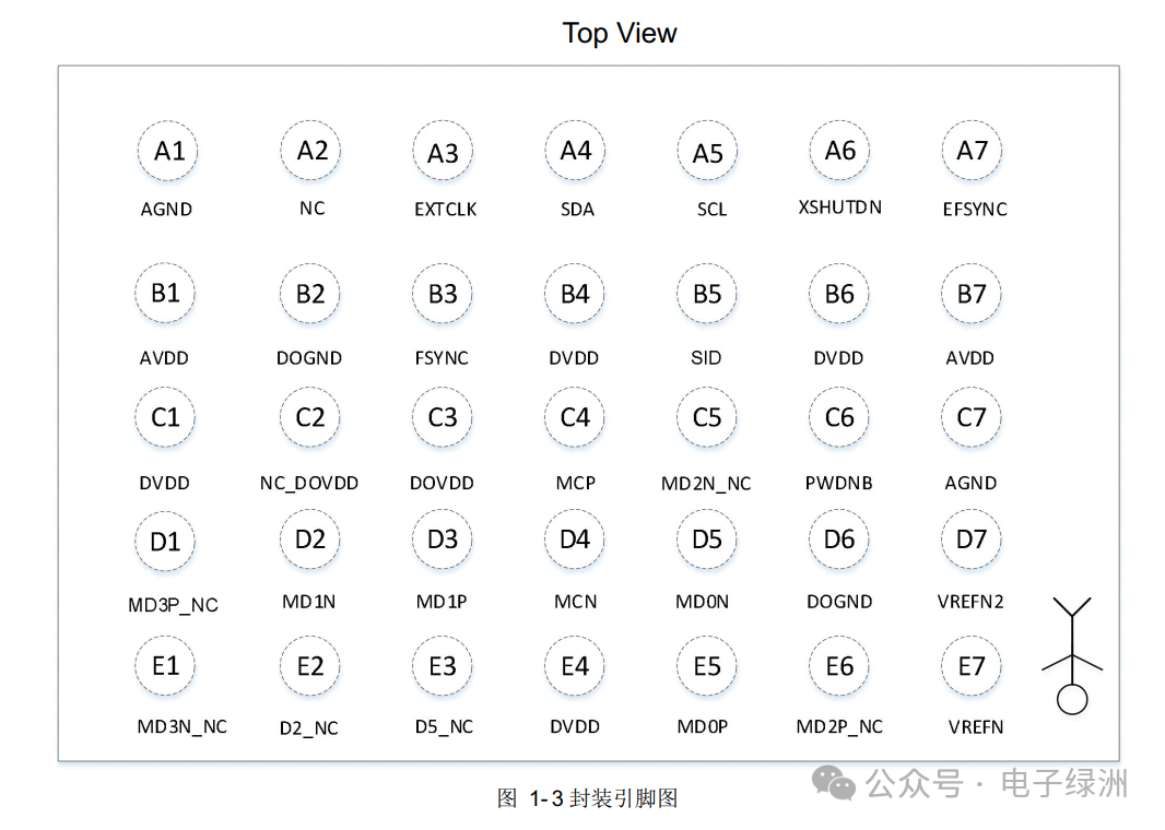
Pinout Diagram:
4. Conclusion
1. The analog voltage of 2.8V can use a high PSRR LDO (PSRR: power supply rejection rate, which is the ripple suppression ratio, input power supply ripple/output power supply ripple) to avoid potential image ripple.
2. The DVDD voltage supplied internally by the sensor is converted from the DOVDD 1.8V voltage through an internal LDO, so the current for DVDD 1.8V is relatively high.
3. SmartSens sensors are all “foot A1”; the imaging direction is opposite to the A1 pin. In contrast, GalaxyCore’s sensor has the A1 pin in the positive direction.
4. The front and back sides of the SmartSens sensor have some boxes that can be used to identify the SmartSens sensor model or the A1 pin.
——END——
In the jungle society, tears are never believed; no amount of complaints will help, and no one will pity you.
Recommended Reading
The Disassembly Series: The 10 Million Dual-Camera Monitoring D220 under the Yingzi Brand
Stop calling me “Engineer X”! The surname of an engineer is very important!
In-depth Discussion: The Return Current Path of Differential Pairs
1 GPIO Port Controls 7 States of 2 LED Lights
Hardware Learning: Component Section – Ferrite Core
Like, Share, and RevisitThank you for your “three connections” supportLimited-time free QR code to join the group for more technical and industry information exchange