Source:Learning About Things
Original Author:Long Road Ahead
This article introduces the concept, causes, and known effects of single particles in semiconductor devices.
Overview
We know that charged ions interact with target atoms while penetrating semiconductor materials, generating electron-hole pairs along the ion’s trajectory. This physical process is the root cause of the single particle effect. From a mechanism perspective, the generation of single particle effects in semiconductor devices and integrated circuits goes through three core stages, each with significant differences in physical behavior:
The first is the charge deposition stage of energetic particles. When high-energy particles bombard the sensitive areas of devices, charge deposition occurs through two pathways: one is direct ionization caused by the collision of ions with the device’s substrate material, which causes outer shell electrons of material atoms to escape their binding and form free charge; the other is the generation of secondary particles (such as recoil nuclei, γ photons, etc.) after nuclear reactions with the impacted atoms, which further interact with surrounding materials, inducing indirect ionization and producing additional charge.
The second is the internal transport stage of ionized charge. The movement pattern of deposited free charge within the device is regulated by the characteristics of the regional electric field: in high electric field areas (such as the depletion region of a PN junction), the charge triggered by a single particle is driven by the electric field force and moves rapidly in a directed drift; in neutral areas (such as the substrate body), the charge exhibits random diffusion due to differences in concentration gradients; additionally, in some devices with special structures (such as CMOS image sensors and power devices), ionized charge can achieve multiplicative transport through bipolar amplification effects, significantly enhancing the total amount of charge migration.
The third is the charge collection and interference stage in the sensitive area. When the transported charge is captured by the sensitive area of the device (such as the capacitor structure of a memory cell or the channel area of a logic unit), the transport process of the charge will excite a transient pulse current, which disrupts the original charge balance state of the device, interfering with the core functions of the device and associated units (such as read/write circuits and clock modules), ultimately manifesting as phenomena like logic flips and functional failures, which are characteristics of single particle effects.
As semiconductor processes continue to iterate, the feature sizes of devices shrink from the micron level to the nanometer level, leading to a decrease in the charge storage capacity of semiconductor memory, which results in an exponential increase in sensitivity to single particle ionization effects. This process evolution not only exacerbates the impact of traditional single particle effects but also gives rise to new physical phenomena such as charge sharing and multiple bit flips—under ultra-deep submicron process nodes, the charge generated by a single high-energy particle impact can cross the boundaries of adjacent storage cells, causing multiple cells to flip logic states simultaneously. The frequency of such phenomena has significantly increased, becoming a core issue that requires breakthroughs in the current research on the mechanisms of single particle effects.
Causes of Single Particle Effects
The induction of single particle effects relies on three core physical processes when a single spatially charged particle traverses semiconductor materials: direct ionization by heavy ions in the material, direct ionization by protons, or ionization induced by recoil nuclei generated from nuclear reactions involving protons.
The ionization process originates from the Coulomb interaction between charged ions with a specific effective charge number and the atoms of semiconductor silicon material: during this process, secondary high-energy electrons (δ rays) are produced, which can extend the ionization path through energy loss and photon excitation within an extremely short time frame of 1 to 100 fs, ultimately forming a distinct ionization track structure. In semiconductor silicon material, the average energy required to generate an electron-hole pair is 3.6 eV (1.0 eV = 10⁻¹⁹ J); linear energy transfer (LET), which describes the average energy loss per unit distance of ions in the transporting material, is commonly expressed in units of MeV·cm²/mg. In integrated circuit design scenarios, to compare the physical size of devices with the amount of charge stored at key nodes, the LET unit can be converted through calculations into the amount of charge deposited per unit distance (such as pC/μm or fC/μm). For example, when the LET value of a charged ion is 98.0 MeV·cm²/mg, the amount of charge deposited per unit distance is approximately 1.0 pC/μm.
The generation mechanism of single particle effects in electronic devices and integrated circuits is also closely related to the device process, structure, and circuit response, but the core process remains ionization—high-energy charged particles traverse the semiconductor device material, forming ionized charge deposition through energy loss. It is important to note that the physical charge generation mechanism not only includes the aforementioned ionization process but also encompasses nuclear reaction processes induced by elastic and inelastic collisions. Furthermore, with the widespread application of modern new electronic devices and integrated circuits in spacecraft electronic systems, the charge collection process induced by spatially charged particle ionization, due to its specificity and complexity, continues to attract researchers for in-depth exploration.
Different single particle phenomena have varying generation mechanisms and core processes, but the common foundation of all single particle effects is consistent: either direct ionization by heavy ions in semiconductor materials or direct ionization by protons after generating recoil nuclei through nuclear reactions. In ground simulation experiments, the ionization process can also be simulated using the absorption of specific energy photons by semiconductor materials—such as simulating space single particle effects in a laboratory environment through pulsed laser irradiation.
For electronic devices and integrated circuits, the generation of single particle effects includes four distinct basic processes:
The first process is charge deposition (i.e., the ionization process): after high-energy charged particles strike the sensitive area, they interact with the semiconductor material through Coulomb interactions, causing the electrons of material atoms to escape from the atomic nucleus, forming a distribution of electron-hole pairs on a micron spatial scale;
The second process is charge transport: the electron-hole pairs (carriers) generated by ionization separate through drift and diffusion movements in different regions of the device, such as the channel region and depletion region;
The third process is charge collection at sensitive nodes: the ionization track of charged particles may traverse one or more PN junctions, and the core of this process is to analyze the charge collection characteristics of independent PN junctions (which may be in reverse or forward bias states);
The fourth process is the device and circuit response: its key feature is the minimum charge required to change the state of the sensitive node unit within the device, known as the critical charge Qₙ. The concept of critical charge was initially used to compare the sensitivity of digital circuits to single particle effects, and in practical applications, it can be extended to the sensitivity analysis of other types of single particle effects. As shown in Figure 1, this illustrates the basic processes of single particle effects and their impact on spacecraft electronic device systems.
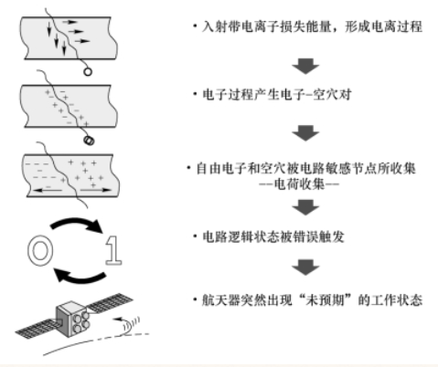
Heavy ions and high-energy protons achieve energy deposition in electronic device materials through the ionization process, forming a dense plasma column of electron-hole pair tracks near the PN junction along the ion’s trajectory. In this track, only a small portion of the ionized charge will recombine, while most of the charge will be captured by the contact nodes of the PN junction; in addition to charge collection near the PN junction, charge can also be collected in areas outside the PN junction through aggregation and diffusion processes, such as completing charge collection in the depletion region of the PN junction through diffusion. The final result of the above charge collection process is the generation of a transient pulse current or transient voltage at the sensitive nodes of the internal circuit along the ion’s impact path.
From the perspective of the generation of single particle effects, the amount of deposited charge formed by charged ions is mainly regulated by three factors: first, the characteristics of the charged ions, including ion energy, ion type, and charge state; second, the physical structure and process characteristics of electronic devices or integrated circuits, specifically covering the effective path depth of charge deposition and the effective path length of charge collection; finally, it depends on the circuit response characteristics of electronic devices or integrated circuits, such as the circuit’s sensitivity to current pulses—this characteristic is closely related to parameters such as the voltage capacitance required for circuit state changes and the circuit response time.
Typically, in silicon-based electronic devices or integrated circuits, the time for charged ions to form deposited charge is within the range of 200 ps. During this time, most of the charge deposited by charged ions will be collected by the sensitive nodes of the integrated circuit, manifesting as transient current pulses or transient voltage pulses at the circuit level. It is worth noting that these pulses also contain a delayed component caused by charge diffusion, which can extend the duration to 1 μs or even longer, and this delayed component is one of the important causes of slow response single particle effects (SEE), such as single particle flips in dynamic memory and latching in CMOS circuits, which are primarily induced by this delayed component.
In the circuit response process of single particle effects, the critical charge Qₙ is the core concept that describes the characteristics of single particle phenomena, defined as the minimum amount of charge required for a sensitive node unit within a digital circuit or integrated circuit to undergo a state change due to single particle effects, mainly used to characterize the circuit characteristics of single particle effect sensitivity. For MOS devices, the size of the critical charge is determined by the distribution parameters of the circuit: first, based on the structural parameters of the device, the barrier capacitance of the sensitive PN junction and gate capacitance can be calculated, and the size of parasitic capacitance can be estimated, then the total capacitance can be obtained based on the series and parallel relationships of capacitance, and the product of total capacitance and the difference between high and low levels is the critical charge—in this case, the critical charge is relatively close to the value of the charge deposited by charged particle ionization. However, for bipolar devices, the difference between the critical charge and the charge deposited by charged particle ionization is more significant. In practical applications, due to the inability to accurately obtain some device parameters, only the distribution range of critical charge can be estimated; additionally, from the perspective of circuit process levels, the parasitic capacitance of sensitive junctions in the same batch of devices also has a variation range, which leads to fluctuations in the critical charge within a certain range.
From the perspective of electronic devices and integrated circuit responses, single particle effects can be divided into two major categories: single event soft errors (SEU) and single event hard errors (SHE). Taking MOS transistors as an example, Figure 2 illustrates the basic physical processes of single particle effects in electronic devices and integrated circuits.
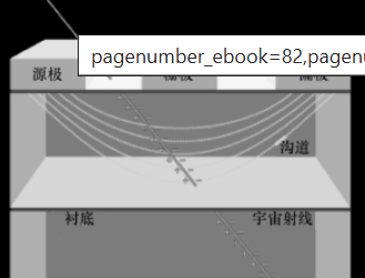
Among them, single event soft errors mainly include single event upset (SEU), single event transient (SET), etc.; single event hard errors encompass single event latchup (SEL), single event burnout (SEB), single event gate rupture (SEGR), etc. With the continuous development of semiconductor device and integrated circuit manufacturing processes, the types of single particle effects have gradually increased. Currently, the main single particle effects discovered in traditional electronic devices and integrated circuits include: single event upset in memory devices, single event transient pulses in analog and digital devices, single event latchup in CMOS devices, single event burnout and single event gate rupture in power devices.
Known Single Particle Effects
In electronic devices and integrated circuits, if the incidence of a single charged particle causes an output signal error in a latch or storage unit, and this erroneous output can be corrected by operating one or more related functional modules of the device, it is determined to be a single event soft error. In addition to the aforementioned single event upset and single event transient pulses, it also includes types such as single event functional interruption. If the incidence of a single charged particle causes irreversible changes in device performance, and this change typically results in permanent damage to one or more modules of the device or even the entire device, it is determined to be a single event hard error, specifically including single event latchup, single event gate rupture, single event burnout, etc. The following is a conceptual introduction to the main known single particle effects.
1. Single Event Upset (SEU)
Single Event Upset is the phenomenon where a single high-energy charged particle (proton or heavy ion) induces a transient signal change, leading to soft errors in electronic devices and integrated circuits. Its physical process manifests as follows: when high-energy charged particles from cosmic space traverse a charge storage unit, they deposit energy in the depletion layer and nearby areas, forming a plasma track column composed of electron-hole pairs; the charge within this track column gathers and is collected at the sensitive node under the influence of the electric field, and if the amount of collected charge exceeds the critical charge value of the node, the state of the storage unit will flip. If the incident particle is a high-energy proton, it will generate secondary particles through inelastic nuclear interactions, and when the charge deposited by these secondary particles along their propagation path meets the collection requirements of the node, it will also change the state of adjacent storage units, causing a flip.
As a soft error, SEU only changes the state of the storage unit without damaging the device and can be corrected by refreshing the data. From the perspective of device applications, SEUs in SRAM often occur within the storage unit, while SEUs in NAND Flash are commonly seen in the floating gate and page buffer of the storage unit. As device processes iterate, the structure of storage units becomes denser, and the distance between adjacent sensitive nodes decreases, leading to a reduction in critical charge values. At this point, the incidence of a single particle may cause two or more adjacent storage units to flip simultaneously, known as single event multiple bit flips. Currently, two types of multiple bit flips have been observed under advanced processes: one is multiple bit flips within a single byte, and the other is simultaneous flips of multiple storage units at adjacent physical addresses. The protective design against such phenomena has become a core technical challenge for the space applications of nanodevices.
2. Single Event Transient (SET)
Single Event Transient is the phenomenon where a single high-energy charged particle (proton or heavy ion) induces voltage/current disturbance signals that propagate within electronic devices and integrated circuits, causing errors. Its induction mechanism is as follows: when high-energy charged particles from cosmic space traverse one or more PN junctions, they deposit energy in the depletion layer and nearby areas, forming a plasma track column of electron-hole pairs; the charge within this column is collected at the node under the influence of the electric field, generating a transient current pulse; when this pulse propagates along the circuit unit link, it leads to erroneous states in the circuit unit. If the incident particle is a high-energy proton, the secondary particles it generates may also deposit sufficient charge along their propagation path and be collected by the PN junction unit, similarly forming a transient current pulse, ultimately causing a change in the circuit state.
SET is a soft error that only changes the state of the circuit logic unit without damaging the device and can be restored by refreshing the logic data. The occurrence areas of SET in different process devices vary: in operational amplifiers and voltage comparators made with bipolar processes, SET often originates from sensitive internal transistors, and the disturbance signal propagates through the transistor link, forming a transient pulse current at the device output to change the circuit state; in MOS digital devices, the SET current mainly arises from the body region and drain region of internal transistors. As device processes become more refined, the critical charge of storage units decreases, increasing the probability of SET occurrence, and its protective design has become a key challenge for the space applications of logic and digital devices.
3. Single Event Latchup (SEL)
Single Event Latchup is the phenomenon where a single high-energy charged particle (proton or heavy ion) traverses the sensitive area of a device, triggering parasitic structures to conduct, thereby inducing an abnormal high current state that leads to device malfunction. SEL is essentially a low-resistance, high-current effect that occurs in parasitic PNPN semiconductor structures, most commonly seen in CMOS devices. Once the device enters a latchup state, it can be maintained with a low voltage, and the large current generated will cause a rapid increase in the internal temperature of the device. If not intervened in time, it may lead to device damage due to overheating; the device can only return to normal state when the supply voltage is cut off to below the latchup critical voltage.
4. Single Event Burnout (SEB)
Single Event Burnout is the phenomenon where a single high-energy charged particle (proton or heavy ion) traverses the sensitive area of a power device, causing parasitic transistors to conduct and triggering an avalanche process, ultimately resulting in an abnormal large current that leads to the malfunction and permanent damage of the MOSFET within the device, classified as a hard error. SEB mainly occurs in power MOSFET devices, and in recent years, similar SEB phenomena induced by heavy ions have also been observed in new high-power devices such as SiC diodes. Its core mechanism is that the large current generated by the avalanche process exceeds the device’s tolerance limit, causing irreversible structural damage.
5. Single Event Gate Rupture (SEGR)
Single Event Gate Rupture is the phenomenon where a single high-energy charged particle (proton or heavy ion) traverses the sensitive area of a device, leading to the breakdown of the MOSFET gate dielectric, causing a permanent short circuit between the gate and drain terminals, increasing gate leakage current, and ultimately resulting in permanent damage to the device, classified as a hard error. SEGR is a common failure in power devices, and similar phenomena can also be observed in NAND Flash devices—especially when heavy ions are incident vertically, the sensitivity of NAND Flash to SEGR significantly increases, posing a serious constraint on the application of advanced process NAND Flash in space or high-radiation environments.
6. Single Event Functional Interrupt (SEFI)
Single Event Functional Interrupt is the phenomenon where the incidence of a single high-energy charged particle (proton or heavy ion) causes partial modules of the device to restart, latch, or exhibit other detectable functional anomalies without needing to repeatedly switch the power supply to restore functionality (which differs from SEL), and does not cause permanent damage, classified as a soft error. SEFI often occurs in complex devices such as microprocessors (CPUs) and digital signal processors (DSPs): when such devices are operational, if a particle-induced flip occurs in internal registers or latches, it can lead to control function anomalies, resulting in functional interruptions. For example, a flip in the internal register of a CPU may cause program execution paths to become disordered, leading to system crashes; if such errors occur in the internal microcontroller of NAND Flash, it may render its controlled programming, erasing, and other operations ineffective.
In addition to the six main types of single particle effects mentioned above, other single particle phenomena, such as Single Event Disturb (SED), have also been observed in ground simulation tests and space flight tests. SED is similar to single event transient pulses, primarily characterized by instantaneous changes in the logic state of digital circuit storage units, and its impact on circuit functionality requires further analysis in specific application scenarios.
END
The reproduced content only represents the author’s views
It does not represent the position of the Institute of Semiconductors, Chinese Academy of Sciences
Editor: Silence
Responsible Editor: Catnip
Submission Email: [email protected]
Previous Recommendations
1. The Semiconductor Institute has made a series of progress in the field of low-dimensional semiconductor polarization light detection
2. From a new star in physics to a pioneer in Chinese semiconductors | History of Science and Technology
3. The Semiconductor Institute has been approved as a “Beijing International Science and Technology Cooperation Base”
4. The Semiconductor Institute has made progress in the research and development of collective guided mode resonance chiral lasers
5. The team of Zhu Lijun from the Semiconductor Institute and collaborators have made significant research progress in the physical origin of anomalous magnetoresistance in magnetic heterojunctions
6. The optical fiber sensing team of the Semiconductor Institute has contributed to the successful convening of the 2025 Disaster Prevention and Mitigation Conference