Table of Contents
[CH.1] Define what Plasma is[CH.2] Please explain the generation mechanism of Plasma.[CH.3] Understanding Paschen’s Law.[CH.4] It is mentioned that energy exceeding the ionization energy must be applied to form plasma. What happens internally if the applied energy is below the ionization energy?[CH.5] Methods to maintain plasma or increase plasma density[CH.6] Can you discuss the characteristics of plasma from an engineer’s perspective?[CH.7] Briefly explain the differences between DC plasma and RF plasma[CH.8] CCP and ICP plasma sources[CH.9] Can we talk about the meanings of CCP and ICP after understanding them?[CH.10] Advantages, disadvantages, and applications of CCP plasma sources[CH.11] Advantages, disadvantages, and applications of ICP plasma sources[CH.12] Differences in the composition of active species in CCP and ICP plasmas[CH.13] Overview of other types of plasma sources
[CH.1] Define what Plasma is.
Plasma is defined as the fourth state of matter. Neutral gas molecules become ionized and dissociated into ions and electrons when they gain electrical or thermal energy. In other words, when high energy is applied externally, collisions occur between atoms, and a large number of electrons are released from the atomic nucleus, forming a collection of various particles, which is the state of Plasma.
※ Hint: The ionization energy of neutral gas atoms (the energy required to ionize them) is as follows: 1. Helium (He): 24.5 eV, 2. Argon (Ar): 15.8 eV, 3. Nitrogen (N): 14.5 eV, 4. Chromium (Cr): 6.8 eV, 5. Neon (Ne): 15.7 eV, 6. Krypton (Kr): 14.0 eV, 7. Xenon (Xe): 12.2 eV, 8. Oxygen (O): 13.6 eV
[1-1] Please further explain the characteristics and roles of the constituent particles that make up plasma.
-
Positive ions: Carrying a positive charge, they play a key role in the generation and maintenance of plasma. Engineers can control their momentum and direction through bias techniques, making them important in dry etching and physical vapor deposition (PVD) sputtering processes.
-
Free electrons: Carrying a negative charge, they are the core particles that maintain plasma neutrality and energy transfer, and their motion characteristics directly affect plasma stability.
-
Free radicals: Electrically neutral but with unpaired electrons, they are highly chemically reactive. Although they cannot be directly controlled by electric fields due to their lack of charge, their concentration in plasma is significantly higher than that of positive ions (note: the actual concentration order is electrons > free radicals > positive ions), and they can be regulated through diffusion effects. This high reactivity makes them advantageous in low-temperature processes, such as plasma chemical vapor deposition (CVD) for interlayer dielectric (ILD) film deposition.
※ Hint: The statement that “the concentration of free radicals is much higher than that of positive ions” is relative; of course, the most abundant particles in Plasma are electrons.
[CH.2] Please explain the generation mechanism of Plasma.
In semiconductor manufacturing processes, plasma is generated through the following mechanism: free electrons gain kinetic energy and are accelerated under the influence of an external electric field (E-Field), colliding with neutral gas particles injected into the reaction chamber. High-energy electrons collide with neutral gas atoms, knocking out their outer electrons, resulting in ionization and the generation of positive ions and new free electrons. The newly generated positive ions move towards the anode under the influence of the electric field, while some positive ions, accelerated by the electric field, collide with the cathode surface and release secondary electrons. This process is known as glow discharge.
The secondary electrons produced are again accelerated in the strong electric field, colliding with more neutral gas particles to cause ionization, triggering a chain avalanche effect. This process continues to cycle, ultimately forming a self-sustaining, high-density plasma.
Therefore, the generation of plasma essentially relies on the secondary electron emission triggered by positive ions colliding with the cathode surface, i.e., the glow discharge mechanism. The formation process can be summarized as follows:
-
Initial free electrons (provided by an external source);
-
Electrons are accelerated in the applied electric field;
-
Accelerated electrons collide with neutral gas, causing ionization and generating positive ions and additional electrons;
-
Positive ions migrate towards the anode in the electric field, with some colliding with the cathode;
-
The cathode emits secondary electrons due to ion bombardment (glow discharge mechanism);
-
Secondary electrons are accelerated and trigger avalanche collisions for ionization;
-
Finally, stable plasma is formed.
Key reverse inferences:
-
The number of secondary electrons generated during the glow discharge phase is far greater than the initial number of electrons, which is crucial for maintaining the self-sustaining nature of plasma;
-
If there is no generation of positive ions and their bombardment of the cathode in step ④, glow discharge cannot occur;
-
To achieve effective ionization, the conditions for gas breakdown must be met, which is fundamentally based on Paschen’s Law, which describes the relationship between breakdown voltage and the product of gas pressure and electrode distance.
[CH.3] Understanding Paschen’s Law.
Paschen’s Law describes the quantitative relationship between the breakdown starting voltage, gas pressure, electrode spacing, and gas type during gas breakdown discharge, providing a theoretical basis for determining the optimal conditions for plasma generation. This law indicates that under certain conditions, the breakdown voltage can be expressed as: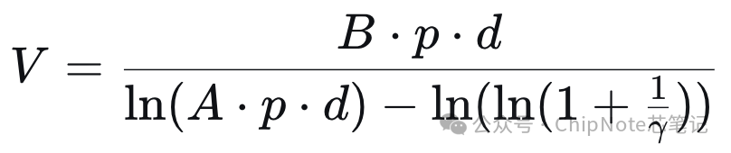
Where:
-
V -
p -
d -
A B K sK should actually be gas-related constants, not a single constant), -
γ
The core of Paschen’s Law points out that the breakdown voltage
Understanding Paschen’s Law is crucial for plasma process control, as it indicates that the following parameters play a key role in discharge:
-
Voltage: Must reach the breakdown threshold for specific gas and structure;
-
Electrode characteristics: Including the secondary electron emission coefficient of the cathode/target material (γ);
-
Electrode spacing: Directly affects the electric field distribution and electron acceleration path;
-
Gas pressure: Affects the average free path of electrons and collision probability;
-
Gas type: Determines constants A and B, as different gases have significantly different ionization energies (e.g., Ar, N₂, O₂).
Therefore, in the design of plasma process equipment (such as etching, CVD, PVD), it is necessary to comprehensively consider gas selection, chamber pressure control, electrode spacing and materials, and the applied voltage to efficiently and stably generate and process plasma.
[CH.4] It is mentioned that energy exceeding the ionization energy must be applied to form plasma. What happens internally if the applied energy is below the ionization energy?
In plasma processes, the applied bias determines the energy of electrons, which in turn triggers different collision physical processes. Taking injected argon (Ar) as an example, its ionization energy is about 15.8 eV. Different ranges of electron energy will lead to the following phenomena:
-
Electron energy < 2 eV: The kinetic energy of electrons is low, and during elastic or inelastic collisions with Ar atoms, energy is mainly converted to thermal energy loss, making it difficult to trigger energy level transitions or ionization.
-
Electron energy in the range of 2 eV ~ 6 eV: Ar atoms absorb energy, and their outer electrons are excited to higher energy levels. Subsequently, during the relaxation process, energy is released in the form of photons, producing light of specific wavelengths.
-
Electron energy in the range of 6 eV ~ 15.8 eV: If the process gas is molecular gas (such as N₂, O₂, CF₄), this energy range may trigger dissociation, breaking molecular bonds and generating highly reactive free radicals. (Note: Argon is an inert atomic gas, with no dissociation process; this is added for accuracy.)
-
Electron energy ≥ 15.8 eV (above Ar ionization energy): Ionization occurs, with electrons completely escaping the atomic nucleus’s binding, producing Ar⁺ positive ions and new free electrons. This process is key to maintaining glow discharge and forming plasma.
It should be noted that in actual plasma, the above processes are not strictly separated but coexist, and their distribution depends on the electron energy distribution function (EEDF). In semiconductor manufacturing, these phenomena are applied in different process stages:
-
Excitation luminescence can be used for plasma spectral diagnostics;
-
Dissociation generating free radicals is used for chemical active reactions (such as CVD film deposition, etching);
-
The ionization process is fundamental to the generation and maintenance of plasma.
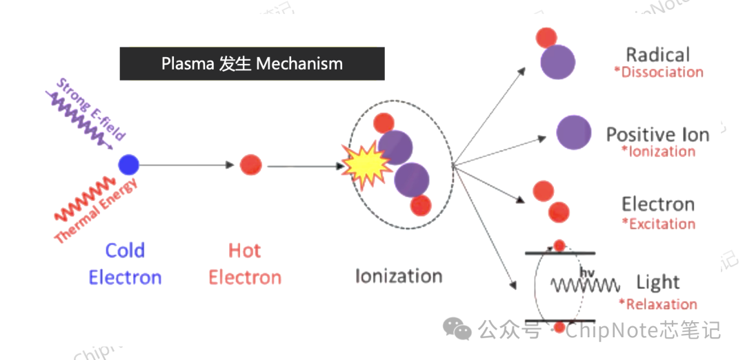
In semiconductor manufacturing processes, the different processes generated by the interaction of plasma with matter have critical process value:
- Excitation: Leads to luminescence phenomena, which can be used for visual or spectral diagnostics of plasma presence. Different substances emit characteristic spectral lines, allowing for profile analysis or achieving endpoint detection (EPD) in etching processes by monitoring changes in the luminescence intensity of specific substances to determine the completion stage of the process.
- Dissociation: Mainly targets molecular gases (such as CF₄, O₂, N₂), breaking chemical bonds to produce highly reactive free radicals. These electrically neutral but highly chemically active particles drive surface reactions in chemical etching (such as dry etching) and chemical vapor deposition (CVD), achieving isotropic etching or low-temperature film deposition, which is the core of the chemical reaction mechanism.
- Ionization: Is the fundamental process for generating and maintaining plasma, with the generated positive ions and electrons being crucial for the process. On one hand, it is a necessary condition for glow discharge; on the other hand, in physical vapor deposition (PVD) and sputtering etching, accelerated positive ions bombard the target or wafer surface, achieving material removal or deposition through physical momentum transfer, dominating the physical process mechanism.
In summary, by controlling electron energy and process parameters, excitation, dissociation, or ionization processes can be selectively utilized to meet the needs of etching, deposition, cleaning, and other semiconductor manufacturing stages.
[CH.5] Methods to maintain plasma or increase plasma density
Based on the particle loss mechanisms in plasma, the following methods can be used to maintain plasma stability or increase its density:
When positive ions are accelerated by the electric field and bombard the cathode surface, they recombine with electrons, leading to ion loss. To maintain plasma stability, sufficient voltage can be applied to maximize the secondary electron emission yield, ensuring that the number of secondary electrons generated exceeds the ion loss, thus maintaining the glow discharge process and achieving self-sustaining plasma.
On the other hand, reducing electron loss can also indirectly increase ion generation efficiency. As described by Paschen’s Law, the chamber gas pressure
In summary, the main methods to maintain and increase plasma density include:
-
Optimizing voltage to enhance secondary electron emission;
-
Adjusting gas pressure and electrode spacing according to Paschen’s Law;
-
Introducing magnetic fields to constrain electrons and improve ionization efficiency.
[CH.6] Can you discuss the characteristics of plasma from an engineer’s perspective?
From an engineer’s perspective, the core of plasma processes lies in its “controllability”, specifically reflected in three actively controllable physical and chemical dimensions:
First, controllability of electrical characteristics. Plasma consists of positively charged ions and negatively charged electrons, whose motion and behavior can be precisely controlled by external electric fields. Engineers can directly influence the energy and directionality of ions by adjusting electrical parameters such as bias, power, and frequency, optimizing the anisotropy of etching or the quality of deposited films, which are the most direct and important control variables in process control.
Second, controllability of magnetic characteristics. By utilizing the confinement behavior of plasma in magnetic fields, engineers can apply magnetic fields (such as those used in ECP and Magnetron Sputtering technologies) to extend electron motion paths, increasing collision probabilities, thereby increasing plasma density. Higher density directly translates to faster etching or deposition rates, while also helping to improve process uniformity and efficiency.
Third, controllability of chemical characteristics. By selecting the type and ratio of process gases and adjusting parameters (such as pressure and power), the concentration and types of active species (such as free radicals and ions) in plasma can be controlled. This directly affects the reaction mechanisms and effects in processes such as reactive ion etching (RIE), plasma-enhanced chemical vapor deposition (PECVD), and surface cleaning, which are key to achieving specific chemical selectivity and reaction process control.
By comprehensively utilizing the control methods across electrical, magnetic, and chemical dimensions, engineers achieve precise optimization of plasma processes, ultimately meeting the stability, repeatability, and high-performance requirements of the processes.
[CH.7] Briefly explain the differences between DC plasma and RF plasma
The fundamental difference between DC (Direct Current) plasma and RF (Radio Frequency) plasma lies in the discharge method and applicable scenarios, as detailed below:
DC Plasma
-
Uses a DC power supply, applying a constant voltage between the anode and cathode, accelerating electrons through the electric field to ionize neutral gas and form plasma.
-
A charge sheath layer forms near the cathode, where sheath voltage accelerates positive ions to bombard the cathode, generating secondary electron emission to maintain glow discharge.
-
Mainly applied in processes involving conductive targets or electrodes, such as sputtering and DC etching.
-
Disadvantage: If the electrode or substrate is an insulating material, charge accumulation (Charging Up) occurs, leading to weakened sheath voltage, unstable discharge, or even termination.
RF Plasma
-
Uses RF AC power supply (typically at a frequency of 13.56 MHz), creating a rapidly alternating electric field that repeatedly accelerates electrons, colliding with gas to generate and maintain plasma.
-
Even on insulating electrodes, a self-bias is formed through the system, generating a DC sheath voltage to sustain glow discharge, avoiding charge accumulation issues.
-
Applicable to various materials, including insulators, widely used in reactive ion etching (RIE), plasma-enhanced chemical vapor deposition (PECVD), and other processes.
-
Advantage: Stable discharge, capable of processing complex structures and insulating samples, with greater process adaptability.
In summary, DC plasma is simple and efficient but only suitable for conductive environments; RF plasma, with its AC drive and self-bias effect, overcomes the limitations of charge accumulation, expanding its application range in semiconductor and thin film processes.
[CH.8] CCP and ICP plasma sources
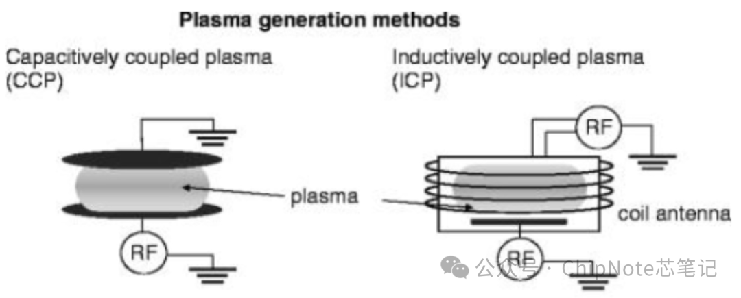
CCP (Capacitively Coupled Plasma) and ICP (Inductively Coupled Plasma) are two mainstream plasma sources in semiconductor manufacturing, with significant differences in excitation principles, plasma characteristics, and process applications:
1. CCP (Capacitively Coupled Plasma)
-
Structure and Principle: Utilizes a parallel plate electrode structure (anode and cathode), applying RF or DC voltage between the electrodes to establish an electric field, ionizing gas to form plasma, belonging to a “diode” type discharge.
-
Characteristics:
-
Plasma density is relatively low (typically 10⁹–10¹⁰ cm⁻³);
-
Ion energy is high (can be precisely controlled by adjusting electrode bias);
-
Good uniformity, suitable for large-area substrate processing.
-
Applications: Mainly used in processes requiring high-energy ion bombardment, such as sputtering, plasma-enhanced chemical vapor deposition (PECVD), and some etching processes.
2. ICP (Inductively Coupled Plasma)
-
Structure and Principle: An induction coil is set around the reaction chamber, with RF current (such as 13.56 MHz) passing through it, generating a time-varying magnetic field that accelerates electrons and collides with gas to form high-density plasma.
-
Characteristics:
-
Plasma density is high (up to 10¹¹–10¹² cm⁻³, 1–2 orders of magnitude higher than CCP);
-
Ion energy is lower and independently controllable (usually requires additional bias voltage);
-
Can stably maintain high-density plasma at low pressures (≤10 mTorr).
-
Applications: Suitable for processes requiring high concentrations of active species and fine control, such as high aspect ratio etching (HAR Etch), metal deposition, and photoresist removal (Ashing).
3. Key Comparisons and Selection Criteria
-
Density and Energy: ICP provides high-density low-energy plasma, suitable for chemically dominated processes; CCP provides low-density high-energy ions, suitable for physically dominated processes.
-
Control Dimensions: The ion energy and density of CCP are strongly coupled; ICP can independently control density and energy through coil power and bias voltage.
-
Process Adaptability: CCP is suitable for scenarios requiring high uniformity over large areas; ICP is more suitable for high precision, high aspect ratio, and low damage processing.
Engineers need to select the appropriate type of plasma source based on process requirements (such as etching selectivity, deposition rate, damage control, etc.) and can develop composite sources (such as CCP+ICP) that combine the advantages of both to achieve more flexible process control.
[CH.9] Can we talk about the meanings of CCP and ICP after understanding them?
Based on the understanding of the basic concepts of CCP and ICP, further distinctions can be made from the perspective of physical mechanisms:
CCP (Capacitively Coupled Plasma) relies on the charge distribution on the electrode surface and the establishment of the electric field. When RF or DC voltage is applied between relatively placed electrodes, a space charge region called “sheath layer” forms on the electrode surface, where a strong electric field exists. The sheath voltage accelerates ions and bombards the electrode, promoting secondary electron emission. These electrons are accelerated by the electric field and collide with neutral gas, triggering and maintaining glow discharge. Therefore, by adjusting the electrode bias, the characteristics of the sheath layer can be effectively controlled, thereby regulating ion energy and plasma density.
ICP (Inductively Coupled Plasma) generates plasma based on electromagnetic induction principles. The coil surrounding the reaction chamber, when RF current (such as 13.56 MHz) is applied, generates a time-varying magnetic field that induces a vortex electric field. Electrons are accelerated in the vortex electric field and gain sufficient energy to ionize gas molecules, forming high-density plasma. It is noteworthy that the RF power applied in ICP is mainly used to drive the coil to generate the time-varying magnetic field, and if independent control of the ion energy incident on the substrate is required, an additional RF bias must usually be applied to the substrate stage to form a controllable sheath electric field.
-
CCP couples energy directly through the electric field between electrodes, with the sheath layer being the key to controlling ion behavior;
-
ICP couples energy through the time-varying magnetic field of the induction coil, achieving high-density plasma generation, with ion energy often requiring additional bias for independent control;
-
Although both use RF energy, the energy coupling methods and core control variables differ, making them suitable for different process scenarios.
[CH.10] Advantages, disadvantages, and applications of CCP plasma sources
CCP (Capacitively Coupled Plasma) sources have unique characteristics in semiconductor manufacturing, with the following advantages, disadvantages, and typical applications:
1. Advantages
-
Simple structure, high ion energy: By applying high voltage between electrodes, high-energy ions can be generated, suitable for etching hard, strongly bonded dielectric films (such as SiO₂, Si₃N₄, etc.).
-
Flexible frequency control, strong process adaptability: Supports RF ranges from low frequency (below 3.2 MHz) to high frequency (13.56 MHz and above). Low-frequency operation can generate high-energy ions, beneficial for achieving anisotropic etching of high aspect ratio (HAR) structures and reducing loading effects.
-
Outstanding anisotropic etching capability: In reactive ion etching (RIE) mode, placing the wafer on the cathode electrode allows for highly anisotropic etching through directional ion bombardment.
2. Disadvantages
-
Relatively low plasma density: Especially under low-pressure conditions, significant electron loss limits plasma density, resulting in relatively low etching rates.
-
Potential substrate damage: High-energy ion bombardment may cause damage, defects, or material modification on the wafer surface.
-
Uniformity challenges: High-frequency operation may lead to uneven plasma distribution due to standing wave effects, affecting process uniformity over large areas.
3. Typical Applications
-
Reactive ion etching (RIE): Achieving selective etching of dielectric and metal films by adjusting electrode bias and frequency.
-
High aspect ratio structure etching (HARC): Utilizing the high ion energy and deep penetration capability of low-frequency CCP to etch micro-nano structures such as contact holes and vias.
-
Compatible with various process configurations: When the wafer is loaded on the cathode, RIE can be achieved; when loaded on the anode (grounded), isotropic plasma etching can be performed.
4. Process Considerations and Selection
-
CCP can suppress macro loading effects at low frequencies, improving uniformity by adjusting gas residence time or using dummy patterns.
-
For RIE lag or inverse RIE lag in micro loading effects, optimizing gas pressure (such as using low-pressure processes to increase the mean free path) and passivation layer control is necessary.
-
Although ICP can provide high-density plasma at low pressures suitable for some HAR etching, CCP remains irreplaceable in scenarios requiring high ion energy and low-frequency control. In process development, a balance must be struck between CCP and ICP based on the target structure’s aspect ratio, material characteristics, and damage requirements.
[CH.11] Advantages, disadvantages, and applications of ICP plasma sources
ICP (Inductively Coupled Plasma) sources are key process equipment in semiconductor manufacturing, with the following characteristics and applications:
1. Advantages
-
High-density plasma generation capability: By applying RF power through the coil to generate an induced electromagnetic field, high-density plasma can be stably generated under low-pressure conditions (typically reaching 10¹¹–10¹² cm⁻³, 10–100 times that of CCP), achieving high etching/deposition rates.
-
Independent parameter control: Plasma density (controlled by coil power) and ion energy (controlled by additional bias) can be independently adjusted, facilitating optimization of selectivity and reducing damage.
-
Suitable for high aspect ratio and fine processes: In high-density plasma chemical vapor deposition (HDPCVD), the sputtering effect can eliminate overhangs, achieving excellent step coverage; it is also suitable for high aspect ratio etching and low-damage surface treatment.
2. Disadvantages and Challenges
-
Initial limitations in plasma uniformity: Due to the electron rotation motion caused by the induced electric field, a ring-shaped (donut-shaped) plasma distribution may form, initially leading to uniformity issues.
-
Higher technical complexity: Requires optimization through antenna design (such as multi-turn coils, planar spiral antennas), frequency modulation, and chamber structure improvements to enhance uniformity, increasing system design and control difficulty.
3. Typical Applications
-
High aspect ratio structure etching: Such as shallow trench isolation (STI), gate etching, and global processing of line width patterns.
-
High-density plasma chemical vapor deposition (HDPCVD): Used for dielectric layer filling, combining deposition and sputtering to achieve conformal coverage.
-
Low-damage surface treatment: Such as photoresist removal (Ashing) and metal etching, relying on high concentrations of active species and controllable ion energy.
4. Technological DevelopmentThrough antenna morphology optimization (such as segmented coils, symmetric designs), multi-frequency driving, and real-time control using artificial intelligence, the uniformity issues of ICP have been significantly improved, and it is now widely used in advanced processes requiring high precision, high throughput, and low damage.
[CH.12] Differences in the composition of active species in CCP and ICP plasmas
Although both CCP and ICP plasma sources are used to generate plasma, there are significant differences in the composition and ratio of active species within them, which directly affects their different applications in processes:
1. Characteristics of species in CCP (Capacitively Coupled Plasma)
-
Lower degree of dissociation: Due to the relatively low plasma density, the average energy distribution of electrons is wide, leading to incomplete dissociation of process gases (such as CF₄, C₄F₈).
-
Rich in polymer precursors: Plasma easily generates larger mass fluorocarbon groups, such as CF₃•, CF₂•, CF•, which have a high tendency for polymerization reactions.
-
Application advantages: Groups like CF₃• and CF• can easily form passivation layers on the sidewalls of etched structures, effectively suppressing lateral etching, thus achieving high anisotropic etching. This is crucial for protecting the sidewalls of patterns during silicon etching or dielectric film (such as oxide) etching.
2. Characteristics of species in ICP (Inductively Coupled Plasma)
-
High degree of dissociation: The high-density plasma and high-energy electron environment allow for complete dissociation of reactive gases, generating a large number of atomic or small molecular high-reactivity groups.
-
Rich in highly reactive etching species: For example, when using fluorinated chemical gases, ICP generates extremely high concentrations of fluorine atoms (F•). F• has strong chemical reactivity, rapidly reacting with silicon to produce volatile products, thus achieving high etching rates.
-
Application advantages: High concentrations of active atoms (such as F•) provide strong chemical etching capabilities, commonly used in processes requiring high selectivity or high etching rates. However, their sidewall passivation capability is relatively weak, often requiring combination with CCP or additional passivating gases (such as CH₂F₂) to achieve anisotropic pattern control.
Summary:
-
CCP: Advantages in generating polymeric/passivating groups (CFₓ), beneficial for sidewall protection and anisotropic morphology control.
-
ICP: Advantages in generating highly reactive etching species (such as F•), beneficial for high-rate chemical etching and high selectivity processes.
-
Collaborative Applications: In advanced etching processes (such as high aspect ratio etching), composite sources of ICP and CCP or stepwise processes are often used, utilizing ICP for main high-speed etching while periodically introducing CCP or passivating gases for sidewall passivation to achieve precise pattern transfer.
[CH.13] Overview of other types of plasma sources
In addition to CCP and ICP, various other plasma sources are also used in semiconductor manufacturing, each with its unique principles and applicable scenarios:
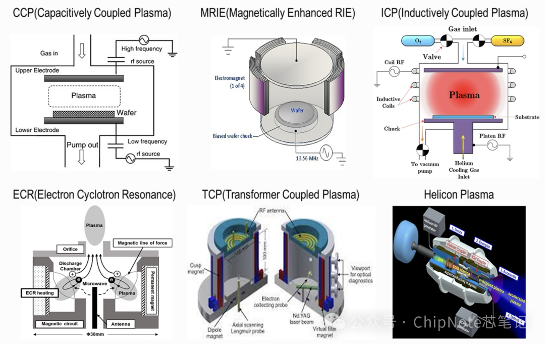
① MERIE (Magnetically Enhanced Reactive Ion Etching)
-
Principle: Introduces a static or low-frequency rotating magnetic field into traditional parallel plate electrode reactive ion etching (RIE) systems, using Lorentz force to constrain electron motion, extending their paths and increasing collision ionization probability.
-
Characteristics: Higher plasma density than traditional RIE, capable of working at lower pressures, enhancing anisotropic etching capabilities, commonly used in dielectric etching processes.
② ECR (Electron Cyclotron Resonance Plasma Source)
-
Principle: By applying a specific strength magnetic field (matching the electron cyclotron frequency with microwave frequency, such as 2.45 GHz) and microwave energy, electrons resonate to absorb energy, being efficiently accelerated and ionizing gas.
-
Characteristics: Can produce high-density, low-electron-temperature plasma, with concentrated ion energy distribution, minimal substrate damage, suitable for low-damage etching and film deposition.
③ TCP (Transformer Coupled Plasma Source)
-
Principle: A flat coil design inductively coupled source, with the RF coil placed outside the reaction chamber window, generating high-density plasma through induced electric field coupling.
-
Characteristics: Simple structure, high plasma density, and independent control of density and ion energy (through bias control), with good uniformity, widely used for etching and deposition.
④ Helical Plasma Source
-
Principle: Uses a helical antenna structure to excite helical waves propagating along the magnetic field, efficiently transferring energy to electrons through wave-particle interactions, forming high-density plasma.
-
Characteristics: Can produce uniform high-density plasma at extremely low pressures (≤1 mTorr), suitable for high aspect ratio etching and advanced device processing.
⑤ HDP (High-Density Plasma) General Concept
-
Definition: Generally refers to plasma with density ≥10¹¹ cm⁻³ (such as ICP, ECR, TCP, helical waves, etc.).
-
Advantages: Good stability at low pressures, high uniformity, and independent control of plasma density and ion energy, with strong process flexibility.
-
Challenges: Narrow process window, high electron energy may increase control difficulty, requiring precise parameter matching.
Summary: Various high-density plasma sources (ECR, TCP, Helical, ICP, etc.) enhance ionization efficiency through different methods, adapting to advanced process requirements such as low damage, high aspect ratio, and high uniformity. Actual selection should consider specific application scenarios and cost-effectiveness comprehensively.
*Content edited by the team. If you are satisfied, please follow me.
Your attention is my motivation. Thank you*
[Second Communication Chip] 5G Era Innovation: The Rise of Next-Generation RF Chips POI-SAW and TF-SAW, Challenging the Dominance of Traditional SAW/BAW Filters!
[Semiconductor Photoresist Materials] Uses and Production Processes of Mask Plates Reticle & PhotoMask
[Semiconductor Lithography Process] Full Process of Lithography Optical High NA Principles, DOF, Process Sequence, Resolution, Wavelength, Pre-bake and Post-bake, Introduction to EUV Processes
[Semiconductor Yield] What is Yield? Process Control Technologies for Improving Yield (Yield)
[Semiconductor Yield] Does Process Shrinking Necessarily Improve Yield? – Understanding Defect Density Used for Yield Prediction
[Semiconductor Cleaning Process] Essential Knowledge Points for Semiconductor Production Processes and Required Cleaning Process Q&A
[Semiconductor Etching Process] The Soul of Semiconductors from 0 to 1 Teaching Etching Processes and Defect Rate Issues for Engineers
[Semiconductor Process] TSMC 2nm Process and Advanced Packaging
[Semiconductor Photoresist Materials] Key Parameter Comparison of i-line vs DUV vs EUV Photoresist Raw Materials
[Semiconductor Yield] What is Yield? Process Control Technologies for Improving Yield (Yield)TH