Many domestic laptop manufacturers use the Quarch M.2 fault injection module to test the fault handling and performance of M.2 SSDs when faced with various exceptions from the host. Of course, server manufacturers or evaluation laboratories also frequently use the Quarch PCIe Gen4/5 card fault injection module for various exception and fault injection tests on the card side; the working principle is the same in both cases. Some friends found the examples of fault injection on M.2 SSDs described in chapter 4.1 of the white paper “PCIe5&6.0, CXL, NVMeNVMoF, SSD, NAND, DDR5, 800GE Testing Technologies and Tools White Paper_ver11.11” difficult to understand, as illustrated in the figure below.
If you find this article helpful and wish to help more people, feel free to share it in your circle of friends or discuss it with friends! We organize these articles and prepare images and video materials. Whether filming videos by setting up the environment yourself or finding excellent third-party videos, along with providing Chinese-English translations, proofreading, and adding subtitle files for everyone’s convenience, these all take a lot of time.
Today we spent an afternoon filming a nearly 40-minute video to introduce and demonstrate the technology of performing various exception and fault injection tests on PCIe Gen4/5 M.2 SSDs in detail. Please watch the video below if interested.
1. Background Introduction
1. Overview of Fault Injection Modules
The fault injection module from Quarch is commonly referred to as the Breaker, and for enterprise-grade SSDs, it can also be called a hot-plug module. Its purpose is to introduce faults in storage device testing to evaluate device performance and reliability.
2. Applicable Device Types
Mainly aimed at enterprise storage devices, such as SAS/SATA disks, PCIe 4.0/5.0 U.2/U.3 disks, and four types of EDSFF disks, which support hot-swapping functionality.
For M.2 SSDs or PCIe cards, sometimes they can be used for power cycling tests; although not typically referred to as hot-swappable, faults can be introduced for testing through these modules.
2. Test Environment Setup
1. Hardware Platform
This demonstration uses an AMD X670E (ASUS motherboard), but an Intel Z790 motherboard can also be used. Note: AMD motherboards have low power issues in M.2 slots or PCIe slots.
2. Connection Method
Connect the Quarch PCIe 4.0/5.0 M.2 fault injection module in series between the M.2 disk and slot.
To facilitate signal observation, connect a SerialTek PCIe Gen5 x 4 M.2 Interposer (including Host Side Adapter and Gen5 POD + host adapter + device adapter) between the Quarch module and the slot. This allows bidirectional signals to be separated and routed to a protocol analyzer for analysis. The signals are divided into U0/U1 (upstream, corresponding to the disk to CPU direction), D0/D1 (downstream), and edge signal SB0 sideband.
3. Testing Process
(1) First Test (No Fault Injection)
1. Preparation Work
Open the analyzer and start capturing data (no data transmission at this time).
Connect to the test host via terminal and use the lspci and nvme list commands to check M.2 SSD device information to ensure proper device recognition.
2. Stress Test Command and Parameters
Use the fio command to perform random read tests on the M.2 SSD, with parameters set to: block size 16K, Number of jobs 30, Runtime 10000 seconds, run for 20 seconds first to observe.
3. Test Results
The PCIe protocol analyzer shows that the stress rapidly increases during the test, with good TLP signals. After 20 seconds, forcibly stop the test, with average read/write operations (IOPS) approximately 455K and bandwidth around 7.1GB/S.
(2) Second Test (Injecting Fault)
1. Quarch Module Configuration
Open the Quarch module configuration interface; we see that the default state is plug (disk connected to host).
In Signal Assignment, signals can be selected by group or signal. Some sideband signals (such as PE wake, PCIe wake, etc., more than 10 in total) allow pull-up and pull-down operations.
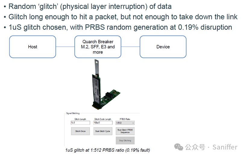
This test focuses on M.2 SSDs (which do not have hot-swappable characteristics, so hot swap-related settings are not applicable), particularly opening the signal glitch function.
Select the receiver end of PCIe Lane 3 (from device to CPU direction) and introduce glitches on the PCIE Receiver Positive and PCIE Receiver Negative signals, setting the glitch occurrence cycle (e.g., 1 microsecond glitch, 10ms no glitch), and adjust the PRBS ratio (it is recommended to try different values; this time set to 512).
Similarly, we select the transmitter end of PCIe Lane 3 (from CPU to device direction) and introduce glitches on the PCIE Receiver Positive and PCIE Receiver Negative signals, setting the glitch occurrence cycle and adjusting the PRBS ratio.
2. Testing Process and Results
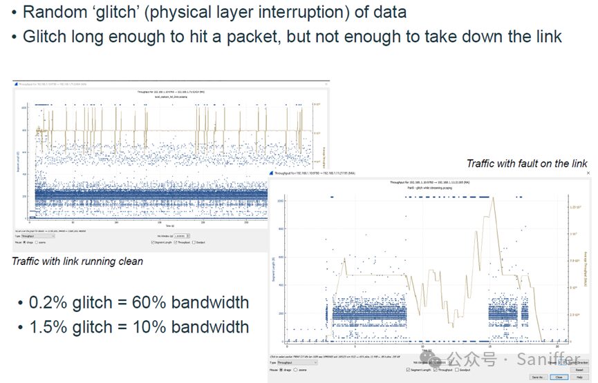
First, start glitch injection, then run the fio stress test command. During the test, numerous errors were found, the FIO process became abnormal, bandwidth dropped to 324 MB/S, and IOPS also significantly decreased, severely affecting data transmission. This was because errors were exported through the fault injection module in the transmit direction (from CPU to disk), causing the disk to need to retransmit data, thus impacting performance.
After stopping the glitch injection, run the fio test again; the bandwidth recovers to about 7.4G, similar to the no fault injection state, proving that fault injection significantly impacts bandwidth, and performance can recover after the fault is eliminated.
4. Summary of Module Functions
1. Pin Connection Simulation
By setting the pins to Source0 (Always off, Disconnected), it simulates poor contact or disconnection of pins, such as issues with certain pins in the M.2 socket or card slot, which can lead to device restarts, dropped disks, or failure to find the device, and can be used to test the device’s handling of abnormal pin connections.
2. Pin Reception Order Simulation (Not Much Effect on M.2)
For disks requiring hot-swappable testing, the pin connection order can be set, but M.2 devices typically do not require this function.
3. Signal Glitch Injection
Glitches can be injected into different signals (such as data signals, clock signals, other sideband signals, and even power signals) to simulate various abnormal situations, such as poor CPU signals or abnormal clock signals during operation (including pulling low into low power or quick reset, etc.), to test the device’s handling of erroneous signals. Glitch characteristics (such as glitch occurrence cycle, PRBS ratio, etc.) can be adjusted, and different settings will have varying impacts on device performance, potentially leading to device drops in severe cases.
5. Precautions and Extended Applications
1. Precautions
During fault injection testing, the FIO process may become abnormal and cannot stop normally; it may need to wait for natural recovery or be handled based on the situation.
Set glitch parameters reasonably to avoid inaccuracies in test results or damage to devices due to excessively frequent or severe glitches.
2. Extended Applications
Scripts can be written to achieve automated testing, facilitating control of pin connections, signal glitch injections, and other operations to improve testing efficiency.
When testing different types of devices (such as disks in laptops, CPUs, etc.), fault injection can be performed on different signal channels (like Lane1 – Lane4) as needed to comprehensively assess device performance and reliability.
6. Get More Information
If you are interested in the testing content, you can download our latest testing white paper from the Saniffer public account, where chapter 4.1 details related content, including the principles of fault injection modules, applications on different devices (like M.2, AIC cards, etc.), and specific test cases (such as the impact of glitch injection on bandwidth).
You can contact relevant personnel to get more support and information about fault injection module testing and applications.
If you have any questions regarding PCIe5&6.0, CXL, NVMe/NVMoF, NAND, DDR5/LPDDR5, and UFS testing, please click “Read Original” in the bottom left to leave a message or message the Saniffer public account, call 021-50807071 / 13127856862, or email [email protected].