
Comprehensive Analysis of Chip Debug Interface Protection Mechanisms
Author | Liu Zheng
Editor | Liu Mengdi
1. Background Introduction
Microcontrollers are the backbone of the modern interconnected world, with widespread applications in robotics, medical devices, aerospace, and automotive industries. With the development of the Internet of Things (IoT), microcontrollers have become even more prevalent in industrial and consumer products. Since microcontrollers perform complex tasks and contain valuable intellectual property that competitors may be interested in, they are worth protecting.
Fault attacks are a type of physical attack that alter the physical environment during the chip’s operation (such as the stability of the clock signal, supply voltage stability, etc.) to affect the chip’s operational process, causing it to malfunction, thus obtaining sensitive information stored in the chip.
Based on this information, Marc et al. from the Technical University of Munich discussed a suppression attack on the FLASH erasure process at CHES 2024, by injecting voltage spikes during the FLASH erasure process, rendering the erasure ineffective and preserving sensitive information stored in FLASH.
2. Prerequisite Knowledge
Modern processors include integrated debug interfaces that assist in development and system debugging. This interface provides access to internal processor components, including FLASH memory. FLASH is often used to store sensitive data such as firmware and cryptographic credentials. Due to the high permissions of this interface, strict constraints must be placed on data integrity and trustworthiness when the chip is deployed in applications.
Some chips can permanently disable the debug interface, while others can enter a restricted debug mode to meet modern development and application needs. As shown in the figure below, the dashed line indicates that only some devices include the corresponding functionality.
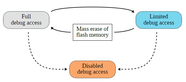
State Transition Diagram of Debug Interface
When the target chip transitions from a restricted debug mode to full debug mode, it undergoes a FLASH erasure process to ensure that sensitive information in FLASH is not leaked. The purpose of this paper is to use fault attacks to invalidate this process, thereby bypassing the debug interface protection mechanism itself to obtain sensitive information from the chip.
The following figure shows the structure of a 1T-NOR FLASH memory cell. This structure is widely used in chips such as the ST series. In the figure, Source is the source terminal, Drain is the drain terminal, Floating gate is the floating gate, Control gate is the control gate, and P-well is the substrate. When a large number of electrons are present in the floating gate, it represents bit 0; when few electrons are present, it represents bit 1.
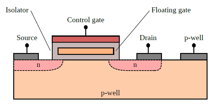
1T-NOR FLASH Memory Cell Structure
For the FLASH Read operation, a reference voltage must be applied to the control gate. If there are no electrons in the floating gate, a current will flow between the source and drain, indicating that the FLASH cell state is logical 1. Otherwise, it indicates that the state is logical 0.
For the FLASH Program operation, a high voltage must be applied to the control gate to attract electrons into the floating gate.
For the FLASH Erase operation, electrons must be removed from the floating gate, typically in three steps: the first step is Pre-program, where all cells to be erased are programmed; the second step is Physical Erase, where an electric field is applied between the control gate and substrate to remove electrons from the floating gate; the third step is Recovery, where for over-erased cells, programming is repeated until they return to normal.
This paper targets the FLASH Erase operation, specifically injecting faults before the Pre-program step to ensure that sensitive information stored in FLASH is not tampered with.
3. Experimental Content
This paper conducted experiments on different models of chips from various manufacturers, performing two types of experiments: voltage spike and electromagnetic fault injection. The voltage spikes were tested using the CW1200 ChipWhisperer-Pro from NewAE Technology platform. The electromagnetic faults were tested using ChipSHOUTER from NewAE Technology platform. The models of the tested chips are shown in the figure below.
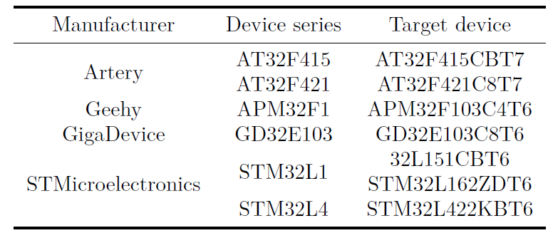
Tested Chip Models
4. Experimental Results
Since the experimental results of several chips were quite similar, this section will use the STM32L422KBT6 as an example for explanation.
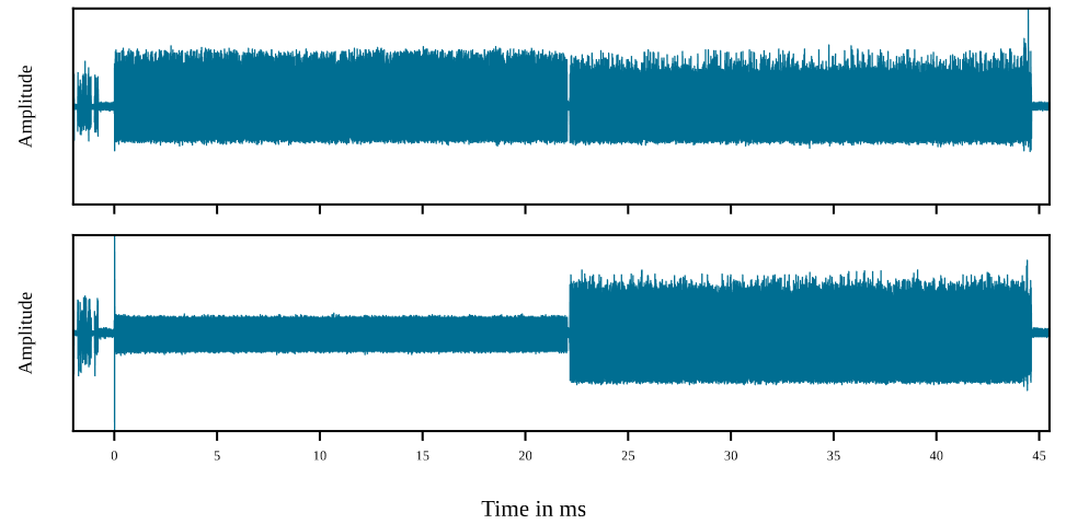
The figure below shows the side-channel energy results of the standalone mass erase process and debug unlock process. It can be seen that the mass erase process is the first half of the debug unlock process; the attack position in this paper is at the beginning of the mass erase process.
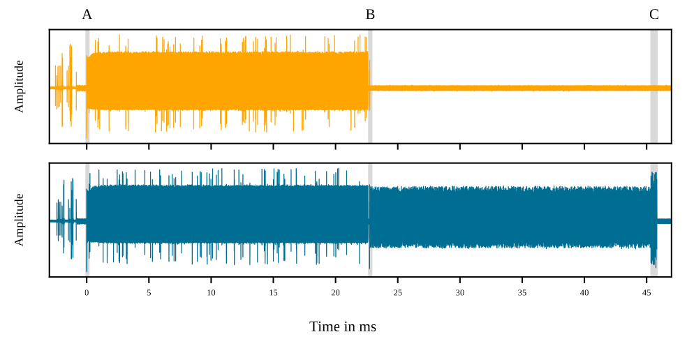
Side-channel energy results of standalone mass erase and debug unlock processes
By magnifying the energy waveforms of sections A, B, and C in the figure above, the following figure can be obtained. Analysis reveals that point 1 is the chip initialization process, and point 2 is the pre-program process. Position B only completes half of the debug unlock process. Point 3 is the erasure process of the security level configuration block, where the pattern at B is similar to A, but shorter, corresponding to the shorter nature of the configuration block. Point C is the reprogramming process for the configuration block.
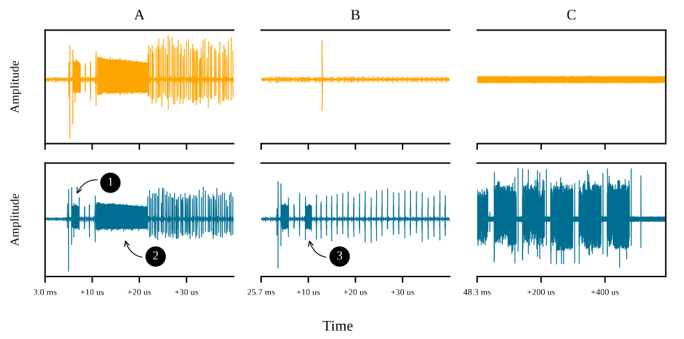
Results of magnified energy waveforms of the debug unlock process
The following image shows an infrared photograph of the back of the STM32L422KBT6 chip after removing the package, where the regular array in the lower left corner represents FLASH, and the high-voltage control circuit for FLASH is on its right.
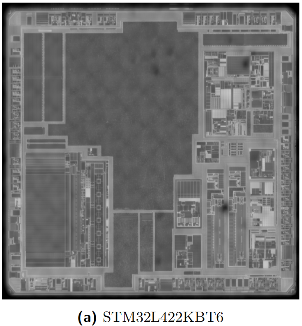
Infrared Photograph of the Back of STM32L422KBT6
The following image shows the failure results, where the upper image is the complete energy waveform during fault injection, and the lower image is the magnified result of the fault injection position. The fault injection position corresponds to position A mentioned earlier, specifically before the pre-program step, where a segment of energy waveform exceeds the range, corresponding to the fault injection position. After fault injection, the energy waveforms of the pre-program and physical erase processes both become very low, indicating that the fault rendered the FLASH erasure process ineffective. Combining basic knowledge of FLASH, it can be speculated that the high-voltage spikes damaged the control circuit of FLASH, rendering the erasure process ineffective.
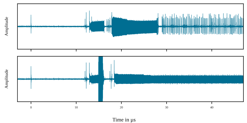
Failure Results of STM32L422KBT6
Conclusion
This paper conducted fault attacks on the FLASH erasure process, rendering the erasure ineffective and preserving sensitive information in FLASH. It should be noted that this attack method is not original to this paper; the main contribution of this paper lies in its detailed analysis of this attack process across multiple chip models, partially explaining the principles of the attack. For results on other chip models and more detailed experimental processes and results, please refer to the original paper.
References
[1] Schink M, Wagner A, Oberhansl F, et al. Unlock the Door to my Secrets, but don’t Forget to Glitch: A comprehensive analysis of flash erase suppression attacks[J]. IACR Transactions on Cryptographic Hardware and Embedded Systems, 2024, 2024(2): 88-129.
Recommended Previous Articles
-
Measuring IPv6 Networks with ICMP Rate Limiting Side Channels
-
Side-channel Template Attack on Ascon Cryptographic Algorithm on 32-bit Devices
-
Content-based Query Password Theft Side-channel Analysis