
Custom semiconductors for high-order harmonic photonics https://doi.org/10.1126/science.aan2395
Abstract:
Thirty years ago, the emergence of high-order harmonic generation techniques in gases laid the foundation for attosecond science and propelled the development of ultrafast spectroscopy of atoms, molecules, and solids. This paper explores high-order harmonic generation in solids through nanostructuring and ion implantation of semiconductors; using wavelength-selective microscopic imaging techniques, we map the distribution of enhanced harmonic emission and observe that the driving field in solids can be locally customized by adjusting the chemical composition and morphology. This enables precise control of high-order harmonic wave fields in finely designed solid targets—this study demonstrates customized high-order harmonic targets for 2-micron laser pulses (harmonic orders up to 9, corresponding to a wavelength of 225 nanometers) and presents an integrated Fresnel zone plate target in silicon, which can self-focus the generated target light field to a diffraction-limited spot size of 1 micron.
Introduction: High-order harmonics generated in gases (1,2) have been used to study electron and ion dynamics on the attosecond time scale (3), providing a means for microscopic studies of atomic and molecular systems (4,5). In recent years, a series of solid systems have also generated high-order harmonics in the visible, mid-infrared (6,7,8), and even terahertz (9) ranges. In solids, high-order harmonic generation is analogous to the “three-step model” of atoms: a strong optical field excites electron-hole pairs, causing them to accelerate and scatter, ultimately radiating higher-energy photons (6,7,9). Besides direct spectroscopic applications (6,8,10,11), solid-state attosecond science offers unique possibilities for controlling high-order harmonic generation. Specifically, “solid-state high-order harmonic engineering” customizes the electronic structure and optical density of states of materials through chemical and structural modifications, such as doping, alloy design, photonic crystals (12), and nanostructures or optical metamaterials (13). The value of engineered high-order harmonics lies in two aspects: first, as a means of actively controlling the generation process; second, as an analytical tool for studying the properties of heterogeneous systems. Thus, the combination of sensitivity to heterogeneous fields and localized field emission (6) provides a unique opportunity that has yet to be fully explored. This paper employs nanostructured zinc oxide (ZnO) and silicon (Si) samples to constrain the driving field and guide emission (Figure 1), while also altering the composition of silicon through ion implantation to adjust the electronic structure of the target material (Figures 1A, C). These two different “customization” approaches (morphology and composition) lay the foundation for a new generation of solid-state high-order harmonic devices—these devices will integrate attosecond physics with optoelectronics and photonics, and the structured targets demonstrated in this study will provide great flexibility for the design of high-order harmonic wave fields. This study uses strong infrared laser pulses with a central wavelength of 2.05-2.3 microns, pulse width of 70 femtoseconds, and repetition rate of 10 kHz, focusing them onto the structured targets and detecting the generated high-order harmonics through spectroscopic methods (as shown in Figure 1D). The peak intensity at the target exceeds 1 terawatt per square centimeter (1 TW/cm²), but does not reach the damage threshold of the structure (the damage threshold is approximately half of this intensity). The grating pattern on the zinc oxide structure (Figure 1B and 1D, “target”; preparation methods are detailed in the methods section) achieves localized enhanced fields through total internal reflection at the cone walls, thereby triggering enhanced harmonic emission at the “hotspot” (Figure 1A). The harmonics are recorded in the far field behind the target (Figure 1D) and focused onto a charge-coupled device (CCD) camera for spatial mapping (“imaging” in Figure 1D). The far-field diffraction patterns confirm that the emitted third (red) and fifth (blue) harmonics exhibit spatial coherence.
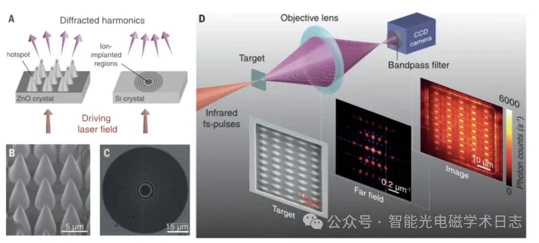
Figure 1: Generation and imaging of high-order harmonics (A) Schematic of nanostructured (left) and ion-implanted (right) semiconductors: the nanocone structure on the surface of the zinc oxide crystal generates diffracted harmonics at the “hotspot” under the action of the driving laser field; the silicon crystal similarly generates diffracted harmonics in the region formed by ion implantation. (B, C) Scanning electron microscope (SEM) images: (B) is a 30° tilted view of the protruding conical structure of zinc oxide (scale bar 5 microns); (C) is the Fresnel zone plate (FZP) pattern formed by ion implantation in silicon (dark regions, scale bar 15 microns). (D) Schematic of the experimental setup: infrared femtosecond pulses illuminate the structured zinc oxide “target”, and the generated high-order harmonics are recorded as “far-field” diffraction signals 5 mm behind the sample (using a tricolor complementary metal-oxide-semiconductor sensor); the photoluminescence background has been subtracted (Figure S2). The bandpass filtered “imaging” of the harmonic distribution is recorded by a high magnification objective (numerical aperture 0.75) and CCD camera.
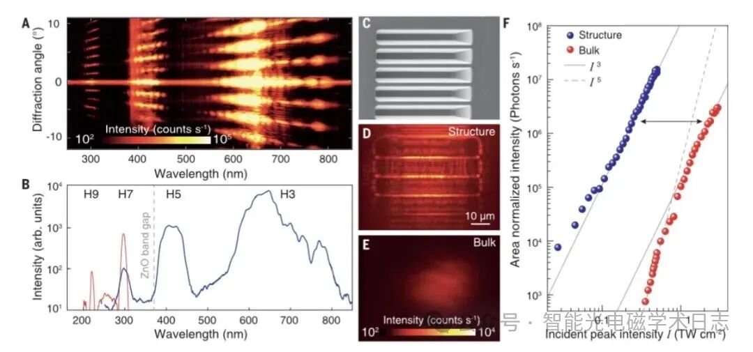
Figure 2: High-order harmonic generation from the zinc oxide structure (A, B) Harmonic spectra generated by the grating structure: (A) is the angle-resolved spectrum (horizontal axis is wavelength, vertical axis is diffraction angle, color represents intensity); (B) is the angle-integrated spectrum (harmonic orders labeled from H3 to H9, “ZnO bandgap” corresponds to its intrinsic bandgap position), excited by 2.05 micron laser (“arb.” is arbitrary units). (C) SEM image of the wedge-shaped grating (30° tilted view). (D, E) CCD images of radiation filtered by a 450 nm bandpass filter: (D) is the signal from the structured sample; (E) is the signal from the bulk sample (scale bar 10 microns), excited by 2.25 micron laser. (F) Intensity scaling of the fifth harmonic signal: signal intensity (normalized to emission area) of structured (blue) and bulk (red) samples as a function of incident peak intensity. The dashed/solid lines represent perturbative/non-perturbative scaling, and the vertical axes of (B) and (F) and all color scales are logarithmic. Figures 2A and B show the harmonic spectra generated by the zinc oxide grating structure (angle-resolved and angle-integrated), which consists of parallel wedge blocks (Figure 2C). We observe that the fundamental frequency (red and blue curves measured by different spectrometers; details in methods section) depends on the harmonic order. Emission from similar structures reflects wavelength-dependent diffraction angles, with the scattered signal near 390 nm (Figures S2~S4) originating from incoherent photoluminescence near the direct bandgap of ZnO (3.37 electron volts at room temperature (14)). Figure 2C shows imaging of the fifth harmonic emission, demonstrating localization and enhancement of the signal (compared to bulk imaging in Figure 2E and videos S2, S3). Figure S5 shows similar imaging results: the most prominent feature is the grating wedge blocks in Figure 2C, with emission confined to approximately 500 nm perpendicular to the wedge blocks, consistent with the geometric structure of field enhancement simulations (Figure 3A). Variations in intensity of the highlighted features may arise from uneven chemical facets (discussed further below). Additionally, we observe stripes around the structure (Figures 2D, S5), which are due to interference between harmonics and the incident/reflected laser fields. Figure 2F shows the relationship between the normalized intensity of the fifth harmonic emission from structured and bulk crystals as a function of incident peak intensity. Based on the imaging hotspot size, we estimate that the emission area of the structure is approximately 25 times smaller than that of the bulk, indicating that the incident intensity required to produce the same signal is much lower for the structure than for the bulk—this suggests that the driving laser intensity at the hotspot is enhanced by at least an order of magnitude (indicated by the arrow in Figure 2F). The fifth harmonic signal from the bulk exhibits a cubic (I³) scaling with laser intensity (perturbative process), while the signal from the structure transitions from fifth to cubic scaling with increasing intensity, with no non-perturbative intensity scaling observed (7). This transition, along with the previously determined intensity enhancement (up to 16 times in simulations, as shown in Figure 3A), collectively demonstrates that the emission from the structure arises from localized field enhancement. Figure 3B plots the normalized fifth harmonic signal from bulk (red) and structured (blue) samples as a function of incident polarization ellipticity (circ=circular polarization; p=p-polarization; s=s-polarization). The bulk signal sharply decreases with increasing ellipticity, consistent with expectations for circular polarization (7,15); while the structured signal shows much weaker dependence on ellipticity, with significant emission even under circular polarization, indicating effective birefringent properties of the structure. At an ellipticity ε=0.6 (corresponding to a vertical phase shift line θ=0, where p and s field components are equal; details in methods section), the normalized bulk signal equals the structured signal under circular polarization, consistent with a 0.17π phase shift caused by polarization-dependent total internal reflection in the structure (16). Furthermore, both experimental and simulated results reveal differences in high-order harmonic signals between the structured and bulk states.
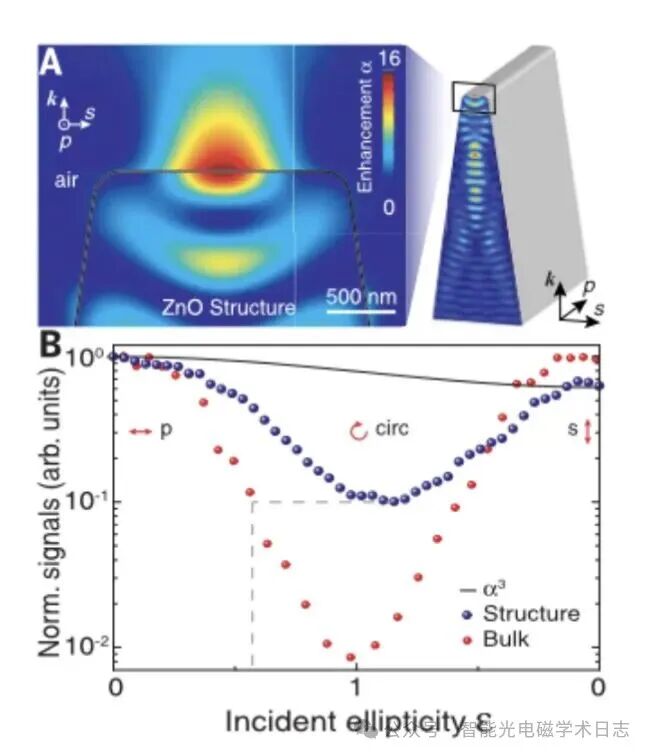
Figure 3: Field simulation and experimental polarization dependence (A) Simulated intensity distribution in a single wedge structure: cross-section perpendicular to the grating grooves, using a circularly polarized plane wave incident along the wave vector k (right side is a schematic), with color representing the field enhancement factor (α). (B) Normalized fifth harmonic signal as a function of incident polarization ellipticity: signals from bulk (red) and structured (blue) samples (“circ” for circular polarization; “p” for p-polarization; “s” for s-polarization), with the dashed line representing α³ scaling.
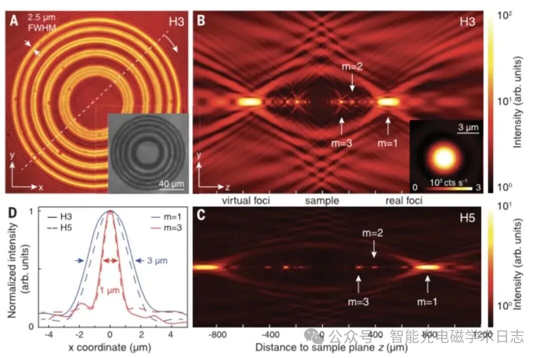
Figure 4: Sources of high-order harmonic generation from Fresnel zone plate patterns (A) Emission pattern of the third harmonic (H3) recorded at the sample plane (z=0 microns), with an inset showing the SEM image of the gallium-implanted Fresnel zone plate pattern in silicon (scale bar 40 microns), “2.5 μm FWHM” represents the full width at half maximum of the fundamental light. (B, C) Focused scans of the third (H3) and fifth (H5) harmonics: the vertical axis scale is related to (A) (the vertical axis of (C) is reduced by a factor of 1.5), with “m=1,2,3” representing the focusing order; (B) inset shows the intensity of the main focus of the third harmonic (scale bar 3 microns). (D) Line profile of the focused intensity: normalized intensity of the third (H3) and fifth (H5) harmonics as a function of x-coordinate, with different focusing orders (m=1,3) labeled.
(Fresnel zone plate) has a diameter of 118 microns and contains 10 zones. Figure 4A shows the emission image of the third harmonic signal from this zone plate, with significantly enhanced emission in the gallium-implanted region; in the spectra produced by such structures, harmonic frequencies can reach up to the 9th order (Figure S6). By moving the objective along the propagation direction (z-axis), we recorded the focused scan results of the harmonic intensity distribution. Figures 4B and C show the third and fifth harmonic signals after azimuthal integration (see the dashed line in Figure 4A), clearly presenting the virtual and real focal points of the zone plate. The line profile (Figure 4D) shows that the focusing width is consistent with the diffraction limit: using a zone plate with a numerical aperture of 0.11 (0.07), diffraction-limited focusing of the third (fifth) harmonics can be achieved. The estimated photon flux of the third harmonic at the main focus (m=1) is approximately 10¹⁰ photons per second (the inset in Figure 4B shows the measured intensity distribution), accounting for the transmission of optical elements and the quantum efficiency of the CCD. In contrast, the photon flux of the fifth harmonic is reduced by a factor of 4; combined with a pulse width of 70 femtoseconds, the peak intensity range corresponding to these photon fluxes is 10⁸ watts per square centimeter. The relative phase information of emissions from the gallium-implanted region and the unmodified silicon region is included in Figures 4B and C. To estimate the phase difference, we used a Fresnel propagator (paraxial approximation; Figure S7) to simulate forward wave propagation, using the integrated intensity distribution of the zone plate at z=0 microns as the initial condition (Figures 4B and C). By adjusting the relative harmonic emission phases of the modified and unmodified regions, we minimized the error between simulated and measured intensities: the phase difference for the third harmonic is π, and for the fifth harmonic is π/3. The origin of the enhancement effect in structured semiconductors is clear—the intensity enhancement of the driving field increases the harmonic yield, but the mechanism of enhancement induced by ion implantation requires further exploration: the implanted gallium ions can act as acceptors, increasing the positive charge density in the valence band; additionally, the implantation process itself introduces various defects (such as vacancies and interstitial atoms), which can also alter the generation process, for example, by adding energy states to adjust the bandgap (17). The phase difference in harmonic emissions between the modified and unmodified regions may reflect changes in the near-surface refractive index induced by carriers; alternatively, the phase shift may arise from changes in the dominant generation mechanism (i.e., from interband transitions to intraband transitions). Regardless of the specific mechanism, our findings have significant implications for advancements in condensed matter ultrafast science and photonics, optoelectronics. High-order harmonics generated in dielectrics in the extreme ultraviolet range (6) can achieve spatial resolutions below 20 nanometers through lensless imaging techniques (18), providing all-optical means to study ultrafast structures and electron dynamics at the nanoscale. As a proof of principle, we applied a phase retrieval algorithm to the far-field diffraction signal of the fifth harmonic (Figure 1D), reconstructing the emission pattern (Figure S8). Combining spectral capabilities (6,8,10,11) with sensitivity to localized fields (8), high-order harmonic radiation will aid in the deeper understanding of active semiconductor devices (such as integrated circuits), providing new methods for the development of next-generation devices in the information technology field. More broadly, the combination of customized semiconductors and plasma nanostructures (19-21) will bring rich applications and foundational breakthroughs in strong-field solid-state physics. As a core outcome of these advancements, this paper demonstrates that high-order harmonic generation in solids can be achieved through engineering techniques, providing possibilities for controlling the spatial distribution, intensity, and phase of high-order harmonic emissions through electronics and nanotechnology. These results fill the gap in silicon photonics and are expected to enable active control of high-order harmonic generation in solids, such as generating extreme ultraviolet light using angular momentum states (22). Fresnel zone plate targets are pioneers for future integrated optical devices and demonstrate that the methods proposed in this paper are a cornerstone of a new branch of optoelectronics—potentially driving the development of compact, electrically controllable solid-state emitters for customized attosecond extreme ultraviolet pulses.
Disclaimer
All images appearing in this article are reprinted; if there are any copyright issues, please contact the author within 20 working days, and we will coordinate to address them (delete according to regulations), and all submissions are the responsibility of the authors.
The public account only shares a platform for scientific research information; submissions and collaborations can be privately messaged to the backend.
The final interpretation rights belong to the “Intelligent Optoelectronic Academic Journal” public account.