
Understanding FPGA clock regions is crucial for achieving high-performance and high-reliability FPGA designs, serving as the fundamental skill in realizing “circuitry in mind” during FPGA development. We can start with a vivid metaphor and then delve into the technical details. Core Metaphor: Think of an FPGA as a cityFPGA chip = a city
Clock region = administrative districts within the city (e.g., East District, West District)
Clock signal = the standard time of the city (e.g., the time broadcast by CCTV)
Global clock network = a high-fidelity broadcasting system covering the entire city, ensuring that every administrative district can hear the time announcement simultaneously and without distortion.
Regional clock network = a local broadcasting system within a specific administrative district, used to distribute the time signals generated within that district.
1. What is a clock region? A clock region is a physical and logical division within the FPGA chip.
Each region contains a certain number of logic resources (such as CLB, BRAM, DSP, etc.), input/output interfaces, and dedicated clock routing and buffering resources.
You can visually see them by checking the layout diagram of the chip in the Device view of Vivado or Quartus, which is usually a crisscross grid.
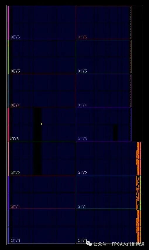
Where XmYn is the clock region coordinate
Main characteristics:1. Fixed physical location
The boundaries and locations of clock regions are fixed at the time of chip manufacturing and are part of the FPGA architecture.
2. Resource independence
Each clock region has its own independent clock entry points, clock buffers, and clock routing resources.
3. Limited quantity
The number of logic resources that a clock region can drive is limited.
This is key to understanding timing convergence.
2. Why are clock regions needed? In early small FPGAs, a single global clock signal could easily drive the entire chip.
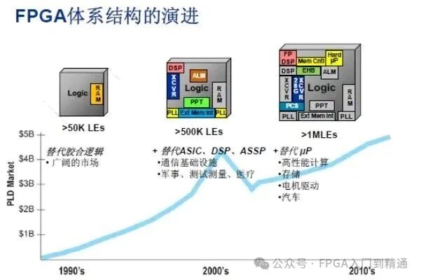
However, as FPGA sizes grow larger (reaching millions or even billions of logic gates), a single clock network faces significant challenges:Clock skew: The delay differences in the clock signal reaching different locations on the chip from the source. The larger the chip, the harder it is to control the skew.
Clock jitter: The uncertainty of clock edges.
Power consumption: Driving a massive global network requires substantial power.
Routing resource contention: If all logic uses a few global clocks, it can lead to routing congestion. The introduction of clock regions is to address these issues:Reduce skew and jitter: By dividing a large chip into multiple smaller regions and using independent, structurally identical clock trees within each region, the clock quality within the region can be greatly optimized.
Distributed power consumption: Distributing clock driving loads across multiple regional clock networks reduces peak power and total power consumption.
Improve reliability: Limits the impact range of a single clock network failure.
Support multi-clock domain designs: Modern FPGA designs often have dozens or even hundreds of clocks, and the architecture of clock regions naturally supports such multi-clock domain designs. 3. Key components of clock regions To understand how clock regions work, it is essential to know several key components within them.
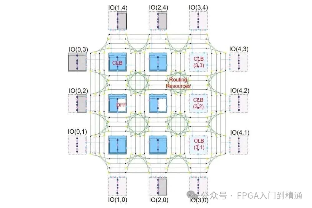
1. Clock pins
Located in the I/O Bank, these are the entry points for external clock signals into the FPGA.
2. Global clock buffers
This is the “backbone” clock driver of the FPGA.
A BUFG can drive all clock regions on the FPGA, but it does so through dedicated entries for each region.
3. Regional clock buffers
This is the “local” clock driver located at the entry of each clock region.
BUFH can only drive its single clock region. It has lower power consumption and higher flexibility.
4. Clock routing
Dedicated metal lines that connect these buffers and ultimately distribute the clock signals to the logic units within the region.
These lines are separated from regular signal lines to ensure performance. 4. Actual workflow of clock regions Assume you have a 100MHz global clock connected to a clock pin of the FPGA. 1. Entering the global network
The clock signal first passes through a BUFG.
2. Distribution to regions
The output of the BUFG connects to the global clock tree leading to all clock regions.
3. Entering the target region
For a specific clock region (e.g., region X) that requires this 100MHz clock, the signal will pass through the entry of that region.
4. Driving within the region
Inside region X, this signal can either be used directly or further optimized through a BUFH for local driving.
5. Serving region logic
Ultimately, this clock signal driven by BUFG (and optionally BUFH) is distributed to all flip-flop clock pins within the region through dedicated clock routing.
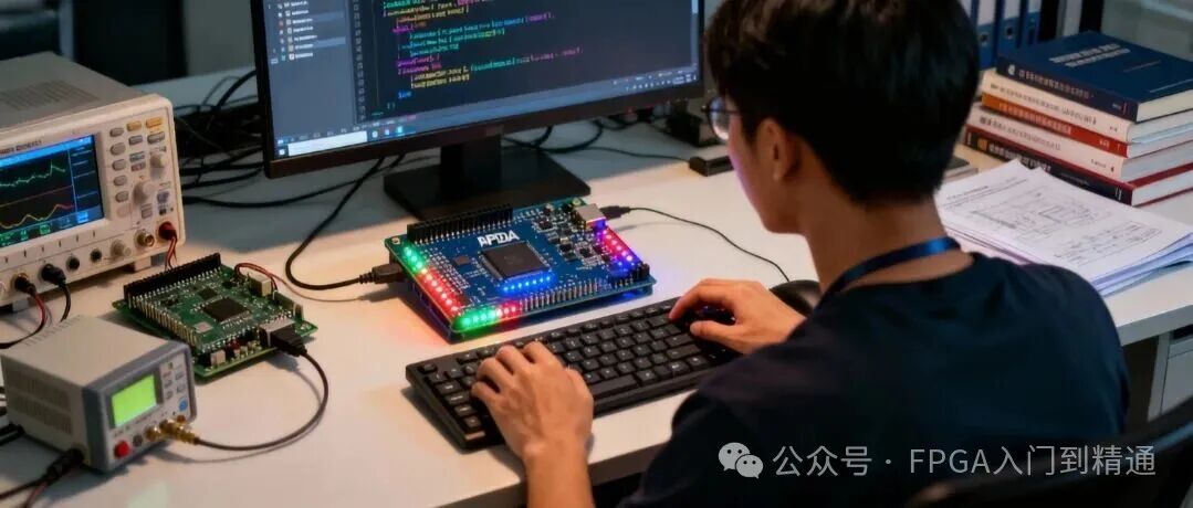
5. Important insights for FPGA designers Understanding clock regions will directly impact your design strategy and timing convergence.
1. Cross-clock domain transmission
Best case: If two interacting logic modules are located within the same clock region, their timing is easily satisfied.
Common case: If they are in adjacent clock regions, the timing is also relatively easy to satisfy.
Challenging case: If they are in diagonally opposite or far apart clock regions, the signal path is long, making setup/hold time violations likely. In this case, careful constraints or pipelining are needed.
2. “Clock region overflow” errors
This is the most common issue related to clock regions.
When a clock signal attempts to drive logic resources exceeding the capacity of a clock region, overflow occurs.
For example: If your clock module instantiates too much logic that cannot physically fit within a single clock region, the tools must use clock resources from adjacent regions to drive them. This introduces greater delays and skews, potentially leading to timing convergence issues.
Solution:
Physical constraints: Use Pblocks to constrain related logic within the same or adjacent clock regions.
Code optimization: Hierarchically and modularly partition the design to make critical modules more compact physically.
Use BUFH: For regional clocks, using BUFH instead of BUFG can reduce power consumption and the use of global resources.
3. Relationship between I/O and clock regions
Each clock region is typically associated with a specific I/O Bank.
This means that the clock and logic interfacing with a certain I/O Bank are best laid out within the corresponding clock region for optimal timing performance. 6. Conclusion Clock regions are a “divide and conquer” architectural strategy adopted by FPGA manufacturers to manage clock distribution issues in ultra-large-scale chips. By dividing the chip into multiple regions with independent clock resources, it ensures clock quality, reduces power consumption, and supports complex designs.
For designers, it is essential to be aware of the relationship between the physical layout of logic and clock regions.
Core design goal: Try to constrain timing-critical paths and logic interacting with specific I/Os within as few adjacent clock regions as possible to avoid “region overflow” and poor inter-region timing.

If you need more learning materials and source code, and want to learn FPGA practical entry and advanced skills, please read the following article: Is FPGA practical entry really difficult? Look here to avoid detours and pitfalls.
Previous readings:
Summary of the “FPGA Basics” series tutorials
Summary of commonly used techniques in Vivado
Summary of FPGA timing constraint series articles
Summary of FPGA book series articles
Summary of FPGA advanced series articles
Summary of FPGA image processing column series articles
How to prepare for FPGA written and interview? (with interview questions download)