1. Experimental Task
-
Task: Based on the STEP-MAX10M08 core board and STEP BaseBoard V4.0 baseboard, complete the design of a serial port monitoring system and observe the debugging results.
-
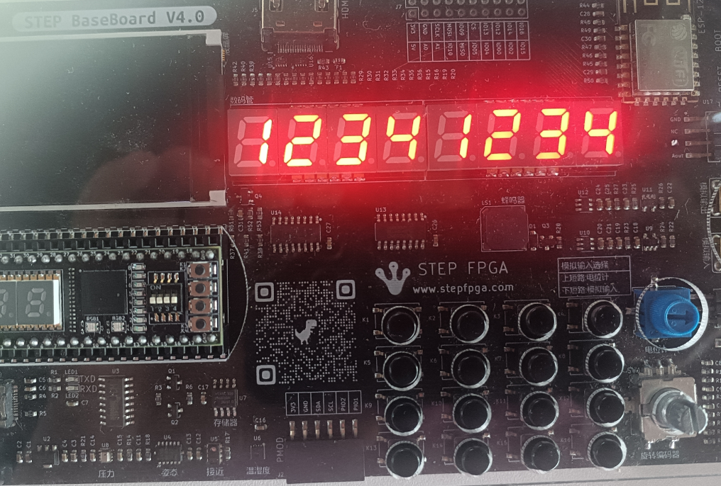
Requirements: Design a serial port monitoring system to monitor the serial port (UART) receiving data in real-time and display the data on the baseboard’s 8-digit digital tube (limited to digits 0~9).
-
Analysis: Drive the CH340 serial communication module on the baseboard through FPGA programming to receive data from PC (serial port debugging assistant) or other serial devices, process it, and finally display the received data on the baseboard’s digital tube through the 8-digit scanning digital tube module.
2.Experimental Purpose
This experiment mainly studies the working principle, protocol, and related knowledge of the serial port (UART) bus, practices how to use FPGA to drive the CH340 module to achieve serial communication design, while reviewing the instantiation application of the scanning digital tube module from the previous section.
-
Familiarize with the working principle and communication protocol of the serial port (UART) bus
-
Complete the design of the serial communication module based on FPGA.
-
Complete the design and implementation of the serial monitoring system
3. Design Block Diagram
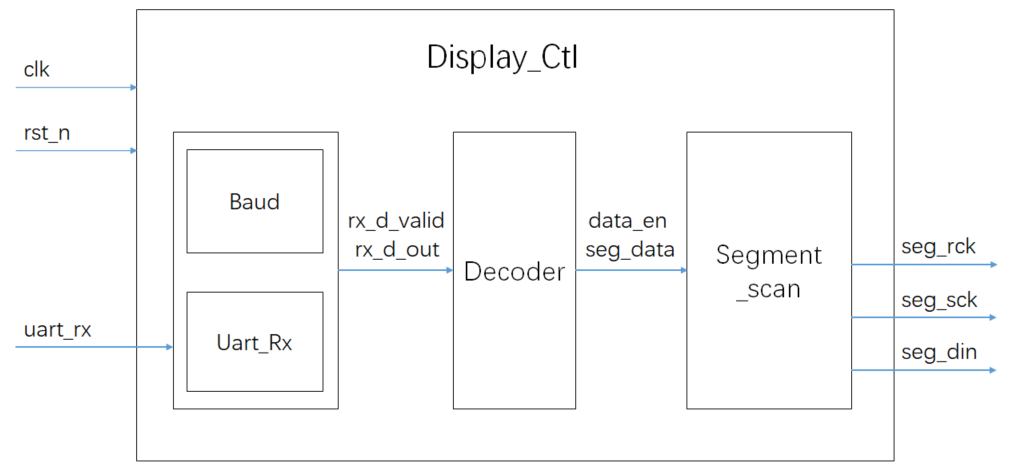
Based on the previous experimental analysis, we can see that this design can be divided into three functional modules:
-
Uart_Bus: UART serial communication design, achieving serial communication data transmission.
-
Decoder: Convert the data received by the UART module into BCD code for display on the digital tube.
-
Segment_scan: Display the data received from the serial port on the scanning digital tube by driving the baseboard.
The top-level module Display_Ctl achieves the overall design of the serial monitoring system by instantiating two sub-modules and connecting the corresponding signals. UART communication is full-duplex, with receiving and sending as two independent designs. This experiment only needs to receive data. There are two key factors in serial communication: transmission format and transmission rate, which can be implemented with two modules:
-
Baud: Control the transmission rate of UART communication data.
-
Uart_Rx: Control the data format of UART communication based on the data transmission rate clock.
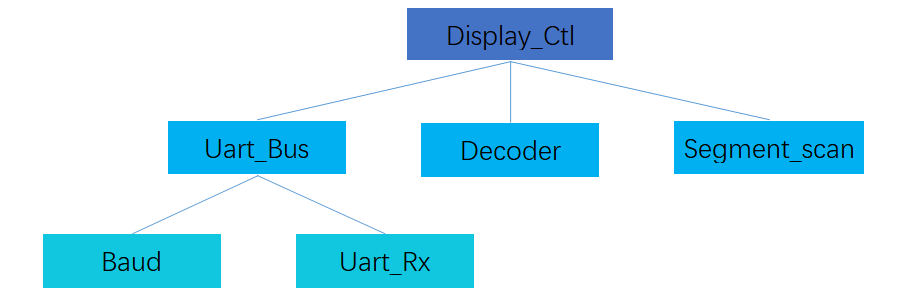
Top-down hierarchical design
Module structure design
4.Experimental Principle
4.1 UART Interface Introduction
UART communication interface
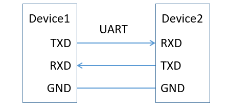
In the embedded field, the serial port generally refers to the UART interface, Universal Asynchronous Receiver/Transmitter (UART), which is a general-purpose serial data bus used for asynchronous communication. This bus supports bidirectional communication and can achieve full-duplex transmission and reception.
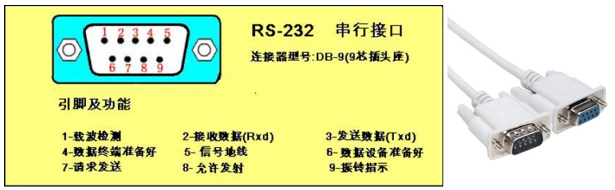
RS232 serial communication interface
In systems or computers, the serial port generally refers to the RS232 interface, also known as COM port or DB9. Older computers and desktops usually have this interface, which has 9 pins, with the three most important pins being: TXD, RXD, and GND. The basic communication logic is completely consistent with UART. To enhance the anti-interference capability of serial communication, the RS232 serial communication interface defines its own voltage standards, using negative logic levels, defining +5~+12V as low level and -12~-5V as high level, which is equivalent to adding a driver to the original UART communication voltage standard to adjust it to the voltage standard of RS232, with the communication principle as follows:
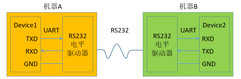
RS232 serial communication
With the development of technology, the types of communication interfaces are increasing, the solutions are becoming more stable, the costs are decreasing, and the sizes are becoming more compact. The RS232 serial communication interface solution is gradually being abandoned, replaced by various faster, more stable, and more compact interfaces. USB is one of the widely used interfaces. To achieve UART communication, a USB to UART solution has been widely applied, with common USB to UART solutions including CP2102, FT232, CH340, etc.
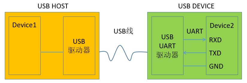
USB to UART communication
Our STEP BaseBoard V4.0 integrates a UART communication module that uses the CP2102 solution. The FPGA drives the CP2102 through the UART bus to achieve data communication between USB and UART, ultimately achieving data transmission between the FPGA and the computer. The timing of UART communication is as follows.
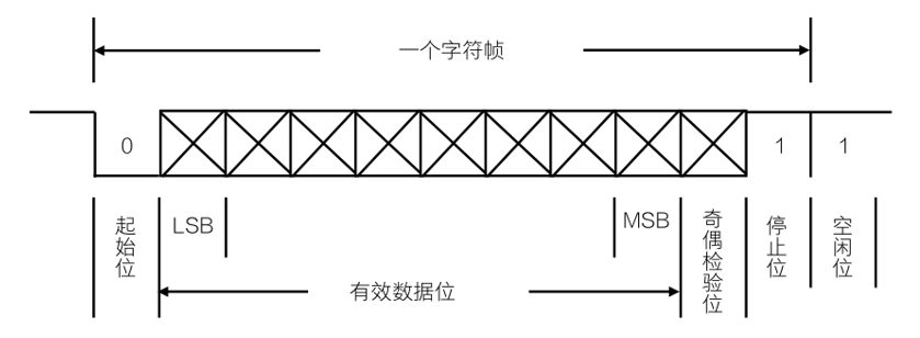
UART communication timing
-
Start bit: First, send a logic 0 signal, indicating the start of character transmission.
-
Data bits: Can be 5~8 bits of logic 0 or 1. For example, ASCII code (7 bits), extended BCD code (8 bits).
-
Parity bit: Adding this bit to the data bits makes the number of 1s even (even parity) or odd (odd parity).
-
Stop bit: It is a character data end marker. It can be 1 bit, 1.5 bits, or 2 bits of high level.
-
Idle bit: In a logic 1 state, indicating that there is no data transmission on the current line.
4.2 UART Module Connection
The circuit diagram of the UART communication module based on the CH340 solution on the STEP BaseBoard V4.0 is as follows:
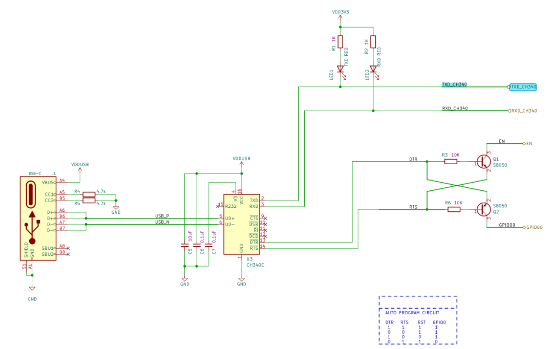
UART communication module circuit
The above diagram is the circuit diagram of the UART communication module based on the CH340 solution, which does not require an external USB communication clock crystal (internally integrated). The CH340 chip TXD and RXD are connected to the FPGA chip RXD and TXD, respectively, and both signals are connected to LED lights, so when UART communication occurs, the corresponding LED lights will flash quickly, serving as the UART communication indicator. The CH340 chip DTR and RTS are connected through two transistors to build a flow control circuit, connecting to the WIFI module ESP8266-12F. When using the UART module to program the ESP8266 module, there is no need to manually enter the firmware programming mode, which will be detailed in subsequent experiments involving WIFI communication; this can be ignored here.
4.3 UART Driver Implementation
|
|
|
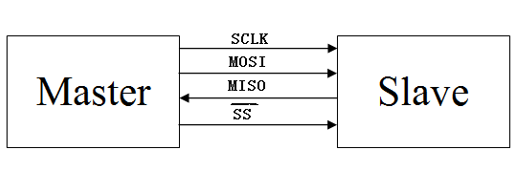
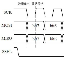
SPI bus connection and timing
|
|
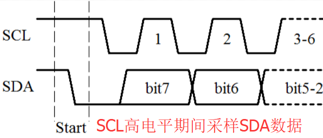 |
I2C bus connection and timing
SPI, I2C, UART bus comparison table:
|
SPI bus |
I2C bus |
UART bus |
|
SS |
SCL |
TXD |
|
SCK |
SDA |
RXD |
|
MOSI/MISO |
|
|
For the SPI bus, both parties complete the bus data sampling triggered by the rising or falling edge of SCK when the bus is enabled, allowing both parties to accurately receive the data sent by the other. For the I2C bus, the receiving party completes the bus data sampling triggered by the high level of SCL. In summary, SCK in the SPI bus and SCL in the I2C bus serve as the clock in communication, with the receiver sampling data based on the corresponding clock state, ultimately ensuring normal communication.
For the UART bus, TXD and RXD are used for sending and receiving data, respectively, equivalent to two independently working single-wire buses. Without the cooperation of a clock line, how does the receiving end obtain the data transmitted by the sending end? There is indeed a method: both parties need to agree on the UART bus data transmission’s communication rate and timing format.
Communication rate:
The data transmission speed of UART is described by the baud rate, which is the number of data bits received or sent by UART per second. For example, a baud rate of 9600 means sending or receiving 9600 bits of data per second, which means the sender needs to maintain the corresponding time for each data bit sent, calculated as follows:
-
1s / 9600 = 1000000us / 9600 = 104.17us
The hardware on the small foot uses a 12MHz clock crystal. If using a 12MHz clock signal as the system clock and using a counter delay to complete UART communication data sampling, the counter delay count terminal value is calculated as follows:
-
12M / 9600 = 1250
Since the baud rate is agreed upon in the protocol, to ensure the universality and flexibility of the protocol, the baud rate parameter has fixed options and cannot be set arbitrarily (if both parties of the UART communication are programmed by themselves, they can define the baud rate they need according to their requirements, except in this case). There are many baud rate parameter options, and you can open the serial port debugging assistant tool to find the baud rate configuration list. The commonly used baud rate values are as follows:
Common baud rates for UART:
|
1200 |
4800 |
9600 |
38400 |
115200 |
Timing format:
Regarding the timing format, it was briefly mentioned in the previous section on the UART interface introduction. The timing during communication is sequentially: start bit, data bits, parity bit, stop bit, idle bit, where the data bits can be 5~8 bits. In this design, we use 8 bits of data, and the parity bit can be omitted. The final determined timing format is as follows:
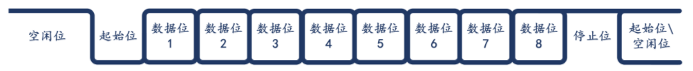
This experiment UART communication timing
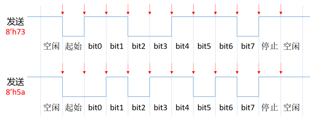
The previously mentioned communication rate and timing format are actually two important parameters in UART communication. The data to be transmitted is output according to the timing format of UART based on the clock of the communication rate, which can be achieved in the following three steps:
1) Combine the data to be sent with the start bit and stop bit to form a 10-bit wide data
2) Use a counter to count delays to generate the timing pulse required for the corresponding baud rate
3) Output the data serially according to the timing (start bit — bit0~bit7 — stop bit)
For example, the timing of sending 8’h73 and 8’h5a through UART, with the red arrows indicating the baud rate corresponding to the timing points.
UART sending data example
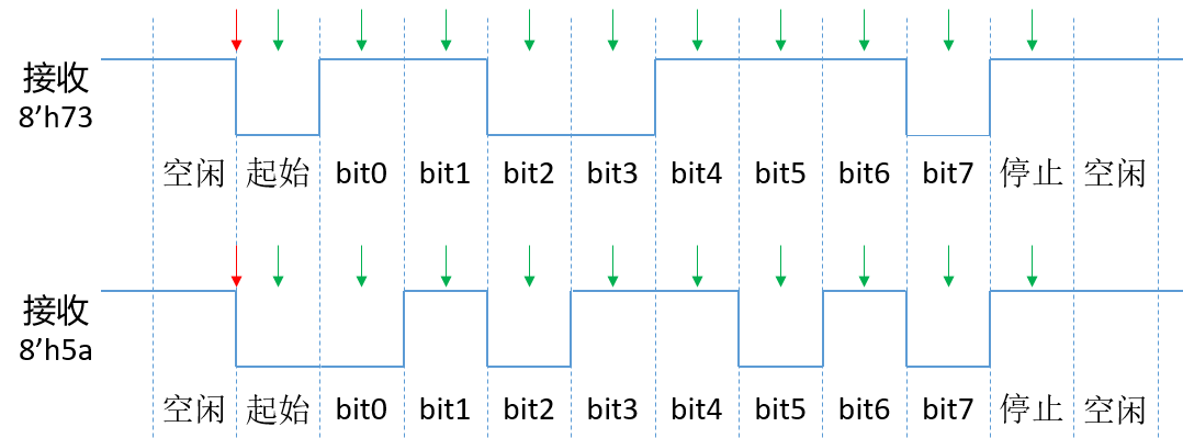
For sending data via UART, the baud rate timing is generated by itself, and the data is actively sent, making the logic relatively simple. However, when UART receives data, since it is uncertain when the other party will send data, it needs to continuously detect the RX signal. When data transmission is detected, sampling can be performed based on the agreed baud rate timing, which can be achieved in the following three steps:
1) Detect the falling edge of the UART RX signal (self-locking, complete reception before unlocking to continue detection)
2) During the reception sampling, the sampling point should be at the middle value of the counter
3) Reassemble the sampled data into 8-bit data according to the timing requirements of UART timing
For example, when the UART RX end receives data 8’h73 and 8’h5a, the red arrows indicate the points where data transmission is detected, and the green arrows indicate the corresponding sampling timing points (the sampling point in the middle of the data is the most stable).
UART receiving data example
Through the above theory, we understand the entire process of sending and receiving data via UART. In both processes, we need the baud rate timing, so we can design a timing module Baud, allowing both sending and receiving to instantiate the timing module to generate the corresponding baud rate timing signal.
Baud module design implementation:
The port program implementation of the Baud module is as follows:
module Baud #(parameter BPS_PARA = 1250 //12MHz clock 1250 corresponds to 9600 baud rate)(input clk, //system clockinput rst_n, //system reset, active lowinput bps_en, //receive or send clock enableoutput reg bps_clk //receive or send clock output);Design a counter to generate the corresponding baud rate timing signal. Since UART may receive data at any time, the timing module must always be on standby, keeping the counter reset, and outputting the timing signal accurately when needed.
The counter design program implementation is as follows:
//Counter counts to meet baud rate clock requirementsalways @ (posedge clk or negedge rst_n) begin if(!rst_n) cnt <= 1'b0; else if((cnt >= BPS_PARA-1)||(!bps_en)) // bps_en=0时,计数器复位 cnt <= 1'b0; else // bps_en=1时,计数器工作,周期为BPS_PARA个系统时钟周期 cnt <= cnt + 1'b1;endWhen bps_en (active high) is enabled, the counter’s counting period is determined by the parameter BPS_PARA. From the previous data reception timing section, we learned that when detecting the falling edge from RX, the counter starts working, and it takes half a timing pulse to reach the data sampling point. For data transmission, it is only necessary to ensure that the time between two adjacent timing points is one counter cycle, so we can generate a pulse signal as the timing signal when the counter reaches the middle value.
The timing signal generation program implementation is as follows:
//Generate the corresponding baud rate clock timing, the receiving module will use this timing for UART data receptionalways @ (posedge clk or negedge rst_n) begin if(!rst_n) bps_clk <= 1'b0; else if(cnt == (BPS_PARA>>1)) //Middle value data stable, make sampling point bps_clk <= 1'b1; else bps_clk <= 1'b0;endSending module design implementation:
The preceding circuit transmits the data to be sent through tx_data_valid and tx_data_in. When tx_data_valid has a pulse signal, tx_data_in is valid data, which is combined with the start bit and stop bit and assigned to tx_data_r, while controlling the timing enable signal to enable and self-lock, then wait until the transmission of 10-bit data is completed before releasing the enable.
The data sending control program implementation is as follows:
output reg bps_en, //Sending clock enableinput bps_clk, //Sending clock inputinput tx_data_valid, //Sending data valid pulseinput [7:0] tx_data_in, //Data to be sentoutput reg uart_tx //UART sending outputreg [9:0] tx_data_r; //Data combined with start and stop bits//According to the completion of receiving data, drive sending data operationalways @ (posedge clk or negedge rst_n) begin if(!rst_n) begin bps_en <= 1'b0; tx_data_r <= 10'd0; end else if(tx_data_valid && (!bps_en))begin bps_en <= 1'b1; //When data needs to be sent, enable the timing enable signal tx_data_r <= {1'b1,tx_data_in,1'b0}; end else if(num==4'd10) begin bps_en <= 1'b0; //One UART transmission requires 10 clock signals, then ends endendUART data sending timing program implementation is as follows:
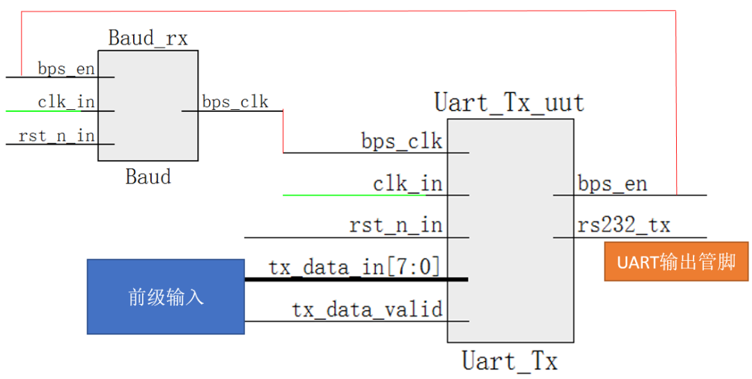
//When in working state, send data according to the sending clock timingalways @ (posedge clk or negedge rst_n) begin if(!rst_n) begin num <= 1'b0; uart_tx <= 1'b1; end else if(bps_en) begin if(bps_clk) begin //Send data according to timing num <= num + 1'b1; uart_tx <= tx_data_r[num]; //Send low bits first, then high bits end else if(num>=4'd10) num <= 4'd0; endendInstantiate and connect the timing module Baud and sending module Uart_tx to complete the design of the sending function, as shown below:
UART sending function design implementation
The receiving module Uart_Rx design implementation:
First, multi-stage buffering is performed on the RX signal to eliminate metastability while detecting the falling edge, with the program implementation as follows:
input uart_rx, //UART receive inputreg uart_rx0,uart_rx1,uart_rx2; //Multi-stage delay latch to eliminate metastabilityalways @ (posedge clk) begin uart_rx0 <= uart_rx; uart_rx1 <= uart_rx0; uart_rx2 <= uart_rx1;end//Detect the falling edge of the UART receive input signalwire neg_uart_rx = uart_rx2 & ~uart_rx1;When a falling edge is detected on RX, enable the timing enable signal, self-lock until the reception operation is completed, and then reset the timing enable signal. The program implementation is as follows:
//Control of the receive clock enable signalalways @ (posedge clk or negedge rst_n) begin if(!rst_n) bps_en <= 1'b0; else if(neg_uart_rx && (!bps_en)) //When transmission is detected, enable the timing enable signal bps_en <= 1'b1; else if(num==4'd9) //Complete UART reception operation, reset the timing enable signal bps_en <= 1'b0; endComplete the data sampling of the UART bus based on the timing signal to obtain 8-bit valid data, with the program implementation as follows:
reg [7:0] rx_data;//When in working state, sample data according to the receive clock timingalways @ (posedge clk or negedge rst_n) begin if(!rst_n) begin num <= 4'd0; rx_data <= 8'd0; end else if(bps_en) begin if(bps_clk) begin num <= num + 1'b1; if(num<=4'd8) rx_data[num-1] <= uart_rx1; //Send low bits first, then high bits end else if(num == 4'd9) begin num <= 4'd0; end end else begin num <= 4'd0; endendWhen the UART reception operation is completed, output the obtained 8-bit valid data to the subsequent circuit, with the program implementation as follows:
//Output the received data while controlling the output valid signal to generate a pulsealways @ (posedge clk or negedge rst_n) begin if(!rst_n) begin rx_data_out <= 8'd0; rx_data_valid <= 1'b0; end else if(num == 4'd9) begin rx_data_out <= rx_data; rx_data_valid <= 1'b1; end else begin rx_data_out <= rx_data_out; rx_data_valid <= 1'b0; endendFinally, instantiate and connect the timing module Baud and receiving module Uart_rx to complete the design of the receiving function, as shown below:
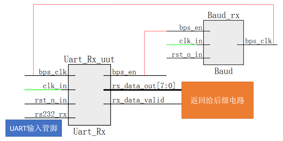
UART receiving function design implementation
The entire UART driver design consists of two independent functional combinations: the sending function part and the receiving function part. The overall design block diagram of UART functionality is as follows:
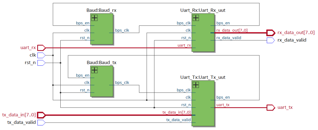
When we need to send data via UART, we only need to instantiate the sending function part design. When we need to receive data via UART, we only need to instantiate the receiving function part design. For example, in this design, the FPGA drives the UART module to receive data sent from the computer’s serial port debugging assistant, so we only need to instantiate the receiving function part design.
4.4 Overall System Implementation
Having just learned about the UART communication module, this design only needs to use the receiving function part design. Each communication will receive an 8-bit data. How to display the corresponding data on the digital tube? First, I need to understand the relationship between the 8-bit data received by UART and the numbers to be displayed.
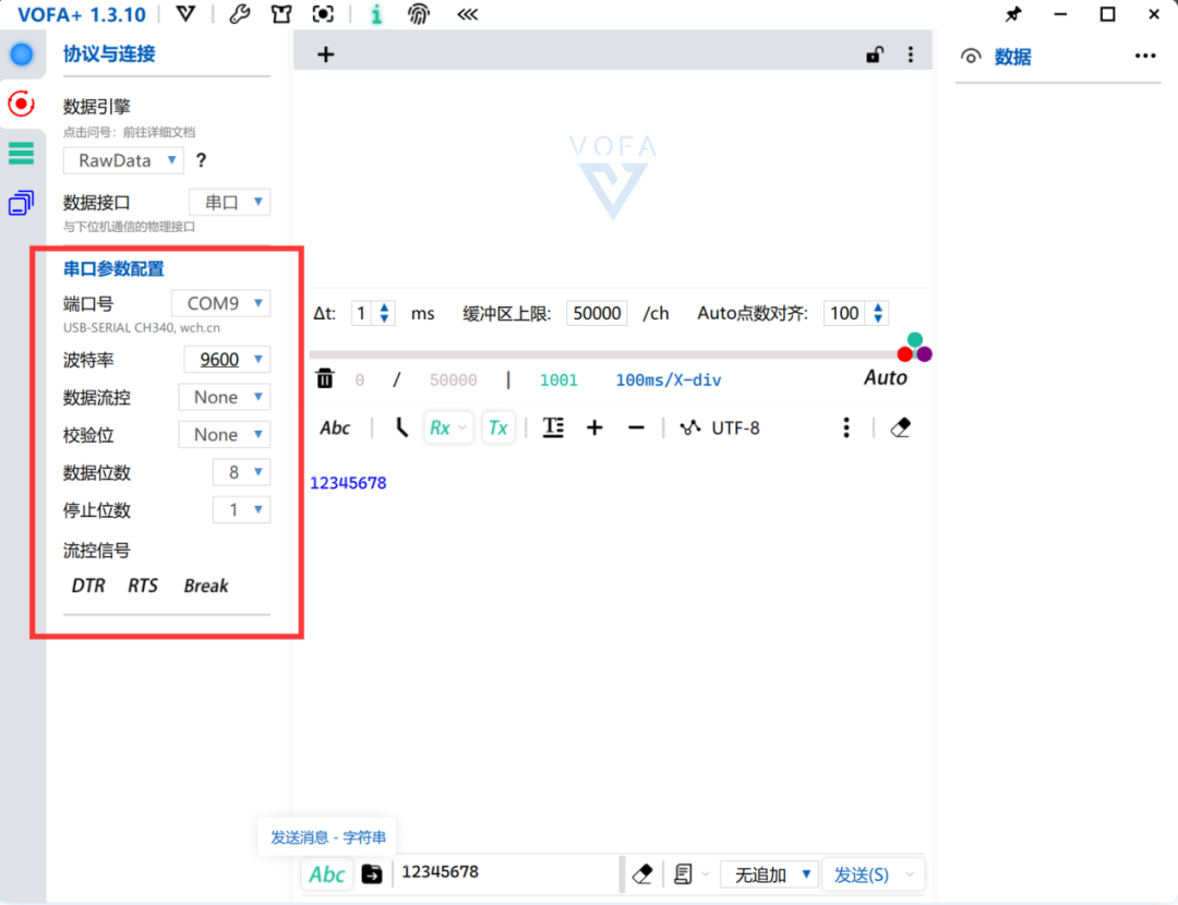
Serial port debugging assistant interface
The above image shows the interface of the computer’s serial port debugging assistant. When we connect the hardware, select the corresponding port in the serial port settings, and configure the baud rate, data bits, parity bits, stop bits, flow control, etc. as shown in the image, click to start establishing a connection. Next, we can input the data to be sent in the serial port sending window, click send, and observe the changes on the baseboard’s digital tube. Re-enter the number, click send, and observe the changes on the baseboard’s digital tube again.