
The basic task of interference immunity design is to ensure that the system or device does not malfunction or lose functionality due to external electromagnetic interference, and does not emit excessive noise interference to avoid affecting the normal operation of other systems or devices. Therefore, improving the system’s interference immunity is also an important aspect of the system design.
 Summary of Circuit Interference Immunity Design Principles
1. Power Line Design
(1) Choose an appropriate power supply;
(2) Widen the power lines as much as possible;
(3) Ensure that the routing of the power line and ground line is consistent with the data transmission direction;
(4) Use interference-resistant components;
(5) Add decoupling capacitors (10~100uF) at the power entry.
2. Ground Line Design
(1) Separate analog ground and digital ground;
(2) Use single-point grounding as much as possible;
(3) Widen the ground lines as much as possible;
(4) Connect sensitive circuits to a stable grounding reference source;
(5) Design the PCB in zones, separating high-bandwidth noise circuits from low-frequency circuits;
(6) Minimize the area of ground loops (the path formed by the return to the power ground after grounding all devices).
3. Component Configuration
(1) Avoid excessively long parallel signal lines;
(2) Ensure that the PCB’s clock generator, crystal oscillator, and CPU clock input are as close as possible, while keeping them away from other low-frequency devices;
(3) Components should be arranged around the core component to minimize lead length;
(4) Implement zoned layout on the PCB;
(5) Consider the position and orientation of the PCB within the chassis;
(6) Shorten the leads between high-frequency components.
4. Decoupling Capacitor Configuration
(1) Add a decoupling capacitor (10uF) for every 10 integrated circuits;
(2) Use leaded capacitors for low frequency and surface mount capacitors for high frequency;
(3) Place a 0.1uF ceramic capacitor for each integrated chip;
(4) Add high-frequency decoupling capacitors for devices that are weak against noise and have significant power changes when turned off;
(5) Do not share vias between capacitors;
(6) Keep decoupling capacitor leads short.
5. Principles for Reducing Noise and Electromagnetic Interference
(1) Use 45° bends instead of 90° bends (to minimize high-frequency signal emissions and coupling);
(2) Use series resistors to reduce the rate of change of circuit signal edges;
(3) Ground the quartz crystal oscillator casing;
(4) Do not leave unused circuit nodes floating;
(5) Clock signals should be perpendicular to IO lines to reduce interference;
(6) Minimize the electric field around the clock to approach zero;
(7) Keep IO driver circuits close to the edge of the PCB;
(8) Avoid forming loops with any signals;
(9) For high-frequency boards, the distributed inductance of capacitors cannot be ignored, nor can the distributed capacitance of inductors;
(10) Power lines and AC lines should ideally be on different boards from signal lines.
6. Other Design Principles
(1) Unused pins of CMOS should be grounded or connected to power through resistors;
(2) Use RC circuits to absorb discharge currents from relays and other components;
(3) Adding a pull-up resistor of about 10k on the bus helps with interference immunity;
(4) Full decoding provides better interference immunity;
(5) Components without pins should connect to power through a 10k resistor;
(6) Keep the bus as short as possible and maintain uniform lengths;
(7) Route wiring between layers as vertically as possible;
(8) Heat-generating components should be kept away from sensitive components;
(9) Route horizontal traces on the front and vertical traces on the back, as long as space allows, the thicker the traces the better (only for ground and power lines);
(10) Ensure a good ground plane, preferably routing from the front and using the back as a ground plane;
(11) Maintain sufficient distance, such as between filter inputs and outputs, opto-isolator inputs and outputs, AC power lines and weak signal lines;
(12) For long lines, add low-pass filters. Keep traces as short as possible, and if long traces are unavoidable, insert C, RC, or LC low-pass filters at reasonable positions;
(13) Use thin traces wherever possible, except for ground lines.
7. Trace Width and Current
(1) Generally, the width should not be less than 0.2 mm (8 mil);
(2) On high-density, high-precision PCBs, the spacing and trace width are generally 0.3 mm (12 mil);
(3) When the copper foil thickness is around 50um, a trace width of 1~1.5mm (60 mil) can carry 2A;
(4) Common ground is generally 80 mil, and special attention should be paid for applications with microprocessors.
8. Power Lines
Keep power lines as short as possible, routing them in straight lines, preferably in a tree-like structure, and avoid circular routing.
9. Layout
First, consider the size of the PCB. If the PCB is too large, the printed traces will be long, increasing impedance and reducing noise immunity, while also increasing costs; if too small, heat dissipation will be poor, and adjacent traces will be easily interfered with.
After determining the PCB size, determine the positions of special components. Finally, layout all components based on the functional units of the circuit.
When determining the positions of special components, the following principles should be followed:
(1) Minimize the length of connections between high-frequency components, and try to reduce their parasitic parameters and mutual electromagnetic interference. Interference-sensitive components should not be too close to each other, and input and output components should be kept as far apart as possible.
(2) For components or wires that may have a high potential difference, increase the distance between them to avoid unexpected short circuits due to discharge. High-voltage components should be placed where they are not easily touched during debugging.
(3) Components weighing over 15g should be fixed with brackets before soldering. Large, heavy components that generate a lot of heat should not be mounted on the printed board but rather on the chassis base of the entire machine, considering heat dissipation. Heat-sensitive components should be kept away from heat-generating components.
(4) The layout of adjustable components such as potentiometers, adjustable inductors, variable capacitors, and micro switches should consider the structural requirements of the entire machine. If adjustments are made inside the machine, they should be placed conveniently on the printed board; if adjustments are made outside, their position should correspond to the position of the adjustment knob on the chassis panel.
(5) Leave space for positioning holes and the positions occupied by fixing brackets on the printed board.
When laying out all components based on the functional units of the circuit, the following principles should be followed:
(1) Arrange the positions of each functional circuit unit according to the flow of the circuit, facilitating signal flow and keeping signals in a consistent direction as much as possible.
(2) Center the layout around the core components of each functional circuit. Components should be evenly, neatly, and compactly arranged on the PCB, minimizing and shortening the leads and connections between components.
(3) For circuits operating at high frequencies, consider the parasitic parameters between components. Generally, components should be arranged in parallel as much as possible. This not only looks good but also makes soldering easier and is conducive to mass production.
(4) Components located at the edge of the circuit board should be at least 2mm away from the edge. The optimal shape for a circuit board is rectangular, with an aspect ratio of 3:2 to 4:3. When the circuit board dimensions exceed 200x150mm, consider the mechanical strength of the circuit board.
10. Wiring
The principles of wiring are as follows:
(1) Wires used for input and output should avoid being parallel to each other as much as possible. It is best to add ground lines between them to prevent feedback coupling.
(2) The minimum width of printed conductors is mainly determined by the adhesion strength between the conductor and the insulating substrate and the current flowing through them. When the copper foil thickness is 0.05mm and the width is 1~15mm, a current of 2A will not raise the temperature above 3°C; therefore, a conductor width of 1.5mm meets the requirements.
For integrated circuits, especially digital circuits, a conductor width of 0.02~0.3mm is typically selected. Of course, if allowed, it is still preferable to use wider traces, especially for power and ground lines. The minimum spacing of conductors is mainly determined by the worst-case insulation resistance and breakdown voltage. For integrated circuits, especially digital circuits, spacing can be as small as 5~8mm if the process allows.
(3) The corners of printed conductors should generally be rounded, as right angles or sharp angles can affect electrical performance in high-frequency circuits. Additionally, avoid using large areas of copper foil, as prolonged heating can cause the copper foil to expand and detach. If large areas of copper foil are necessary, it is best to use a grid pattern, which helps to eliminate volatile gases generated by the adhesive between the copper foil and substrate when heated.
11. Pads
The center hole of the pad should be slightly larger than the diameter of the component lead. If the pad is too large, it may lead to cold solder joints. The outer diameter D of the pad should generally not be less than (d+1.2)mm, where d is the lead hole diameter. For high-density digital circuits, the minimum pad diameter can be taken as (d+1.0)mm.
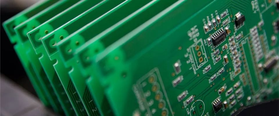
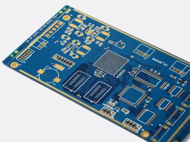
12. PCB and Circuit Interference Immunity Measures
The interference immunity design of printed circuit boards is closely related to the specific circuit. Here, only a few commonly used measures for PCB interference immunity design will be explained.
13. Power Line Design
Based on the current size of the printed circuit board, try to increase the width of the power lines to reduce loop resistance. At the same time, ensure that the routing of the power line and ground line is consistent with the direction of data transmission, which helps to enhance noise immunity.
14. Ground Line Design
The principles of ground line design are:
(1) Separate digital ground from analog ground. If the circuit board contains both logic circuits and linear circuits, they should be kept as separate as possible. The ground for low-frequency circuits should ideally use single-point parallel grounding; if actual wiring is difficult, partial series grounding can be used before parallel grounding. High-frequency circuits should use multi-point series grounding, and the ground lines should be short and wide, with a grid pattern of large area ground foil around high-frequency components.
(2) Ground lines should be thickened as much as possible. If the ground line is too thin, the ground potential will change with current variations, reducing noise immunity. Therefore, the ground line should be thickened to handle three times the allowable current on the printed board. If possible, the ground line should be at least 2~3mm thick.
(3) Ground lines should form closed loops. For printed circuit boards composed solely of digital circuits, grounding circuits arranged in a loop can generally improve noise immunity.
15. Decoupling Capacitor Configuration
One of the conventional practices in PCB design is to configure appropriate decoupling capacitors at various critical points on the printed board.
The general principles for decoupling capacitor configuration are:
(1) Place a 10~100uF electrolytic capacitor across the power input. If possible, using a capacitor greater than 100uF is better.
(2) In principle, each integrated circuit chip should have a 0.01pF ceramic capacitor; if space on the printed board is insufficient, a 1~10pF capacitor can be placed for every 4~8 chips.
(3) For devices that are weak against noise and have significant power changes when turned off, such as RAM and ROM memory devices, decoupling capacitors should be directly connected between the chip’s power and ground lines.
(4) Capacitor leads should not be too long, especially for high-frequency bypass capacitors, which should have no leads.
 END
END
Disclaimer:This article is reproduced from the internet, and the copyright belongs to the original author. If there are any copyright issues, please contact us in a timely manner. Thank you!