

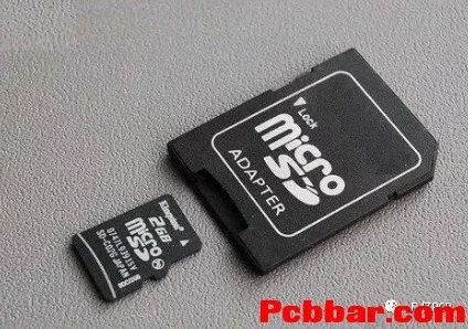
Micro SD Card is a very small flash memory card, originally created by SanDisk. This memory card was initially called T-Flash and later renamed Trans Flash; it was renamed to Micro SD because it was adopted by the SD Association (SDA). Other memory cards adopted by the SDA include Mini SD and SD cards.
Its primary application is in mobile phones, but due to its small size and increasing storage capacity, it has also been used in GPS devices, portable music players, and some flash storage drives. It measures 15mm x 11mm x 1mm, approximately the size of a fingernail, making it the smallest memory card available today.
It can also be connected to an SD card slot using an SD adapter. Currently, MicroSD cards offer capacities of 128MB, 256MB, 512MB, 1G, 2G, 4G, 8G, 16G, 32G, 64G, and 128G (during the MWC 2014, SanDisk broke the traditional maximum capacity of 64GB by officially releasing a Micro SD XC card with a capacity of up to 128GB.
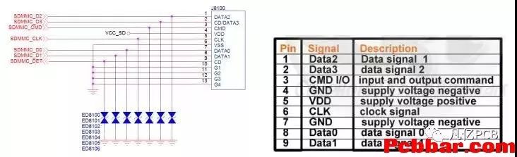 (SD Card Pin Definition)
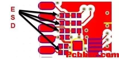
SD cards are frequently inserted and removed, so the design must consider the addition of ESD protection devices.
1) The capacitor for VCC_SD needs to be placed close to the card slot pins for filtering, following the principle of starting with larger capacitors and then smaller ones.
2) The TF card should be placed as close to the edge of the board as possible for easy insertion and removal, and ESD devices should be placed near the TF card. The wiring should go through the ESD device before entering the SD card, without using through holes, as shown below.
3) The SD card wiring should be single-ended, controlling the impedance to 50 ohms;
4) All signal lines should ideally be routed on the same layer to ensure signal consistency. Keep the routing away from high-frequency signals, and if space permits, ground each line individually. In tight spaces, a group grounding approach can be used, ensuring there is a complete reference plane for routing;
5) The clock signal for the SD card should maintain a distance of about 20 mil from other signal lines, and if space allows, grounding should be applied;
6) The data lines within a group should not differ too much, ideally controlled within 400 mil, and the total wiring length should be kept under 12.5 inches to improve stability and compatibility.
7) All signal lines for the SD card should have equal lengths, using the clock line as the target, with a tolerance of within 300 mil.
I hope the above sharing can help with your learning.


Countdown to 618 shopping festival, exciting courses not to be missed.
I hope these tips can help with your learning.

● This article helps you understand the development history of ROM/RAM memory.
● Top PCB engineers vs ordinary PCB engineers.
● Common specification requirements in PCB design.
● 10 difficulties in microcontroller circuit design are all here!
Fan Yi Education
Teacher Zheng Zhenyu
Long press to recognize and add the teacher’s WeChat.