
As the industry accelerates towards 800G Ethernet and optical interconnects, engineers face new challenges in managing electromagnetic interference (EMI) at unprecedented speeds while ensuring signal integrity. The shift to 112G Pulse Amplitude Modulation 4 (PAM4) SerDes technology not only brings faster edge rates and denser spectral content but also significantly increases the risk of radiated and conducted emissions.
At the same time, compact module form factors (such as QSFP-DD and OSFP) compress high-speed transmission channels, DC-DC converters, and control circuits into tight spaces, increasing the potential for crosstalk and noise coupling. Power transmission noise, insufficient shielding, and poorly designed return paths can cause an 800G design that works successfully in the lab to fail EMI radiation tests due to non-compliance.
To avoid unexpected issues in the later stages of product development, it is essential to systematically address EMI issues starting from the PCB level, balancing high-speed signal integrity with practical manufacturability in stacking, routing, and grounding decisions.
This article will provide engineers with actionable PCB design strategies to reduce EMI in 800G systems while maintaining high performance in data center and telecommunications environments.
Layout Considerations
For chip-to-chip 112G PAM4 transmission, the critical frequency is the Nyquist frequency, which is half of the baud rate. Since PAM4 encodes 2 bits per symbol, we have:
-
Baud rate = half of the bit rate. For example, 112 Gbps / 2 = 56 Gbaud.
-
Nyquist frequency = 56 Gbaud / 2 = 28 GHz.
For 112G mid-range PAM4 transmission, the maximum insertion loss at 29GHz should be kept below 20dB. Megtron 7 material has a loss factor (Df) of only 0.003 at 29GHz, which is classified as “very low loss,” making it highly suitable for 112G applications. The lower the Df value, the less energy loss the material incurs, allowing the original signal strength to be effectively transmitted to the receiving end.
This helps maintain the critical amplitude differences between PAM4 levels, thereby reducing the bit error rate (BER). In contrast, low-cost FR-4 material has a Df value of about 0.015 at this frequency, which is too high for 112G PAM4.
Hole Size and Shielding Performance
To avoid EMI, it is crucial to understand the relationship of wavelengths during design, especially when wires or openings may unintentionally act as antennas. Joints, gaps, or holes in EMI shielding can act as slot antennas. When the size of these openings approaches a significant proportion of the interference signal wavelength, they can become effective radiation sources, allowing EMI to escape and potentially leading to failures in anechoic chamber tests.
The general design guideline is that the maximum size of any opening should be less than 1/20 of the wavelength (λ) of the target highest frequency to ensure shielding performance. Figure 1 shows common ventilation openings and shielding ventilation structures used in airflow management.
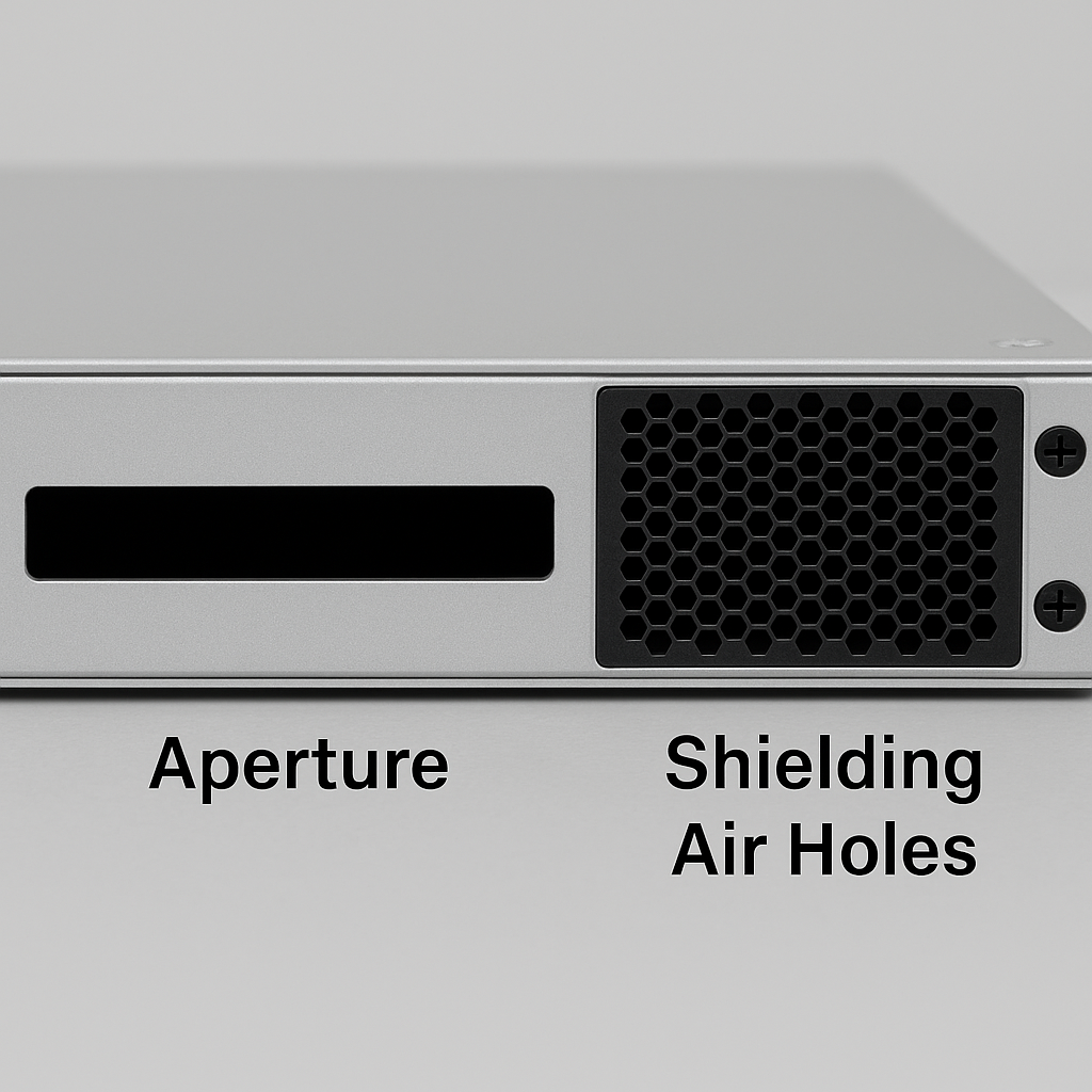
Figure 1: Ventilation holes and shielding design applied in airflow management.
The wavelength calculation formula is λ = c / f = (3 × 10⁸) / (28 × 109) = 10.7 mm Maximum opening size = λ / 20 = 0.536 mm
Therefore, for devices operating at 28GHz or susceptible to 28GHz interference, all opening sizes should ideally be less than 0.536mm. As frequency increases, the allowable opening size will further decrease.
Routing Guidelines and the Impact of Via Stubs in 112G PAM4
In 112G PAM4 designs, the spacing rules between two sets of differential pairs differ depending on whether it is TX to TX or TX to RX. Generally, compared to lower-speed designs, the allowable serpentine trace length for 112G PAM4 is shorter. For weakly coupled differential pairs, serpentine traces have less impact on the signal.
The so-called “via stub” refers to the unused portion of a through-hole that extends beyond the signal transition layer (see Figure 2). For example, if a signal enters an inner layer through a via from the top layer, the excess portion extending to the bottom of the PCB forms a stub.
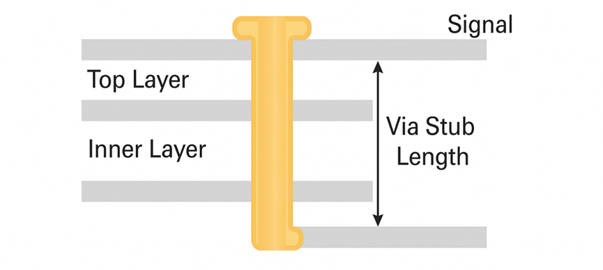
Figure 2: Schematic diagram of PCB via stubs.
f = c/(4 × L × √ℇeff) f = Resonant frequency of via stub = 28 GHz c = Speed of light = 3 x 10⁸ m/s L = Length of via stub = 1.533 mm = 60.35 mils ℇeff = 3.05 at 28GHz
In Megtron 7 material, a via stub of about 60 mils will resonate near 28GHz. For 112G PAM4 designs, this length is too long and can cause serious signal integrity issues.
Power Considerations
Generally, 800G optical modules consume between 13W and 18W per port in short-distance applications, with specific values depending on the module manufacturer’s datasheet. These optical modules contain 8 channels of 112G to achieve 800G transmission. For a 1RU device, if equipped with 32 QSFP-DD, a 25.6T switch is required. Figure 3 shows a simplified schematic of a 1RU device with a single ASIC.
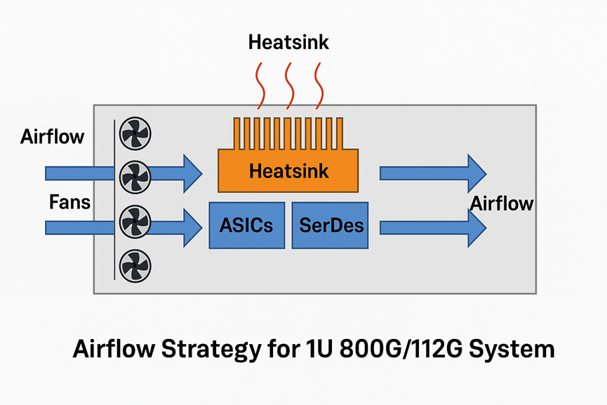
Figure 3: Airflow management schematic for a 1U high-speed system using a single ASIC.
The power consumption of 112G PAM4 SerDes is quite high (typically 0.5–1.0 W per channel). In the worst-case scenario, power consumption = 8 x 1 W = 8 W.
Assuming T_case_max = 90℃, T_ambient_max = 50℃, then Rth = (90 – 50) / 8 = 5° C/W. System designers must ensure that the heat sink and thermal interface materials can provide ≤ 5°C/W thermal performance.
Q = Power to be dissipated (watts), ΔT = Allowable temperature rise of the system (℃), conversion factor = 3.16.
Airflow (CFM) = Q × 3.16 / ΔT = 2000 × 3.16 / 15 = 421
In 1RU, engineers typically use multiple high-speed (PPM) fans of 40 × 40 × 56 mm for airflow distribution, with each fan providing about 25–30 CFM. The required number of fans = 421 / 25 = 16.8 ≈ 17 fans. Due to external power supplies occupying rear space, installing this many fans can be quite challenging.
Design Recommendations
As 800G hardware and 112G PAM4 SerDes become the standard for next-generation data centers and telecommunications systems, engineers must address multiple design challenges in high-density 1RU systems: maintaining signal integrity, controlling EMI, and managing stringent thermal constraints.
Careful selection of PCB materials (such as low-loss Megtron 7), precise routing to minimize via stub resonance, and strict control of opening sizes to ensure shielding performance are key to avoiding signal degradation and EMI test failures. Additionally, the high power density of 800G optical modules and SerDes requires advanced thermal design, airflow planning, and redundancy design to meet operational and reliability goals.
Systematically addressing EMI and thermal management issues early in the design process will enable engineers to confidently create 800G systems that can pass certification tests and maintain high performance in real-world operating environments. This not only avoids costly late-stage redesigns but also ensures robust deployment and long-term operation of high-speed systems in evolving application scenarios such as cloud and AI.
Editor: Ricardo