
Author

John Watson is a professor at Palomar College in San Marcos, California.
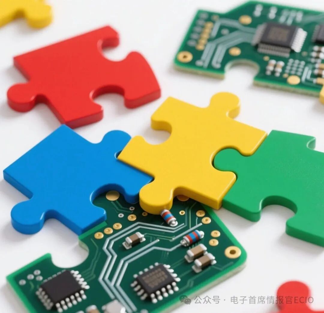
People often ask me, “Can you design a perfect PCB?” At first glance, the answer seems to be yes. After all, if you follow all the rules, double-check, and use professional tools, you should achieve perfect results—right?
I often use a puzzle as a metaphor for PCB design: it is a large and complex puzzle game, but the key difference is that there is no unique solution, but rather countless possible solutions. In fact, PCB design is trickier than a puzzle because the shapes of the pieces can change at any time during the assembly process.
Even more challenging is that PCB design contains both static and dynamic information. Static information remains fixed, while dynamic information is associated with the design and continuously changes. As you might expect, changes in dynamic data can have catastrophic effects on the design.
While this article focuses on output data, having a grasp of the overall design is equally important. There is a parent-child cascading relationship at various stages of PCB design: the component library is the parent of the schematic, the schematic is the parent of the PCB design, and the final output files are their children. Therefore, seemingly minor errors in the design process can often evolve into significant defects due to this cascading effect.
The “control circle,” “influence circle,” and “concern circle” theory proposed by Stephen R. Covey in his classic work, “The Seven Habits of Highly Effective People,” perfectly aligns with our discussion. As Covey explains, the “control circle” encompasses all matters you can directly control—those factors that affect the success or failure of your work; while the “influence circle” includes things that, although uncontrollable, can be indirectly influenced through controllable factors.
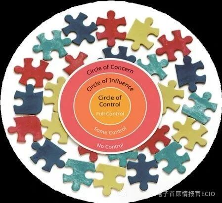
For PCB designers, your “control circle” includes the core areas for which you must take full responsibility: ensuring that the schematic and layout files are clear and complete; maintaining an accurately updated bill of materials (BOM); rigorously checking all traces, pad stacks, and 3D models; detailing layer structures, drilling parameters, and tolerance requirements; performing design rule checks (DRC) for error correction; adhering to corporate specifications and industry standards; establishing a version control system to maintain file traceability; and writing clear design documentation—these are the core competencies that PCB designers must hone, and they are key to winning in your “control circle.”
On the other hand, the troublesome “influence circle” involves aspects that you can only influence but cannot directly control. The design data package is a typical example—such as the manufacturing capabilities: even if you design a circuit board that is deemed perfect and complete all verification steps, if the factory’s equipment cannot achieve it, all is in vain. Different manufacturers have significant differences in processing equipment and process tolerances.
Maintaining close communication with manufacturers is crucial. When should you communicate? The answer is: throughout the entire project lifecycle. From before the design starts, during the development process, to every stage after delivery, you should maintain seamless contact with the process engineers; this close collaboration should even reach the level of being “inseparable.”
Any worthwhile PCB manufacturer possesses three levels of process capabilities: standard, intermediate, and advanced. More importantly, quality manufacturers will also provide design for manufacturability (DFM) guidelines—these rules clarify key parameters such as trace spacing and component hole sizes, essentially transforming the “influence circle” into a “control circle” through standardized requirements.
Component availability is a typical “influence circle” issue when creating a data package, yet it often becomes the biggest challenge faced by designers. It is entirely beyond the designer’s control and can cause PCB design projects to stall. Component availability is a challenge for every designer.
The causes of component shortages are complex: components that are immediately available for purchase may suddenly face stockouts, extended lead times, discontinuation notices, or price surges. Even if the PCB layout is perfect, if the manufacturer cannot obtain the specified components, production cannot proceed. This dilemma often leads to project delays, cost increases, and even forces engineers to redesign using alternative components.
Incredibly, some engineers neglect to check the stock status and lead times of components during the design phase. More commonly, components that are available for purchase during the design phase may be out of stock by the time production begins—this mismatch between supply and demand is particularly frequent when market demand is high.
To bring this risk back into the “controllable circle,” it is recommended to check the stock status of components before starting the design, confirming real-time inventory and lead time data through authoritative platforms like Digi-Key and Mouser; prioritize using standard generic components, as these not only have stable supply chains but also offer better procurement prices and shorter lead times.
Another practical tip is to add alternative components (often referred to as substitute part numbers) to the bill of materials (BOM). These alternative components must meet two key conditions: functional parameters must match completely, and package sizes must be identical. When the preferred components are out of stock, alternative options can be immediately activated without affecting production schedules.
Designers can also establish early communication mechanisms with the procurement team to stay informed about which components are easy to procure and which are high-risk materials. For critical components (such as microprocessors, power modules, etc.), it is advisable to implement a pre-material strategy, suggesting small batch procurement during the design validation phase.
Engineers should also avoid components that are nearing obsolescence. It is recommended to use component lifecycle management tools to monitor the status of components in real-time. Before final production, all components must undergo a secondary verification—this simple recheck process often helps avoid sudden supply chain risks.

Designers need to be proactive when creating design data packages, not reactive. If you only respond to a situation or a problem, it is too late. The best way to shift something from the designer’s influence circle back to their control circle is to take action early and be prepared. This means thinking ahead, asking the right questions, and checking important details before problems arise.
Excellent design data packages require forward-thinking rather than passive responses. Taking action only when problems arise is too late; true professionalism lies in establishing preventive mechanisms and building responsive systems. It is recommended that designers read “The Seven Habits of Highly Effective People.”

END








Above are the electronic chief intelligence officer partners(partial)
Order does not indicate priority