
With the development and application of microelectronics technology, flexible thin-film transistors with characteristics such as bendability, deformability, and portability have attracted extensive research in fields such as wearable health management devices and flexible displays. Flexible thin-film transistors made of metal oxides, although they have better performance and stability compared to transistors made from carbon nanotubes and organic materials, and can be compatible with semiconductor processes for large-scale fabrication, their higher temperature annealing processes can negatively impact the performance and stability of flexible substrates and transistors. Therefore, exploring flexible thin-film transistors with ideal device performance at low temperatures (200°C or lower) is of considerable significance.
Al₂O₃/HfO₂ Nanolaminate Dielectric Boosting IGZO-Based Flexible Thin-Film Transistors
Qiuwei Shi, Izzat Aziz, Jin-Hao Ciou, Jiangxin Wang, Dace Gao, Jiaqing Xiong, Pooi See Lee*
Nano-Micro Letters (2022)14: 195
https://doi.org/10.1007/s40820-022-00929-y
Highlights of This Article
1. A stable stacked Al₂O₃/HfO₂ insulating layer was developed through atomic layer deposition at a relatively low temperature of 150°C.
2. A bottom-gate top-contact flexible thin-film transistor (TFT) was further fabricated on a flexible substrate with an Al₂O₃/HfO₂ insulating layer.
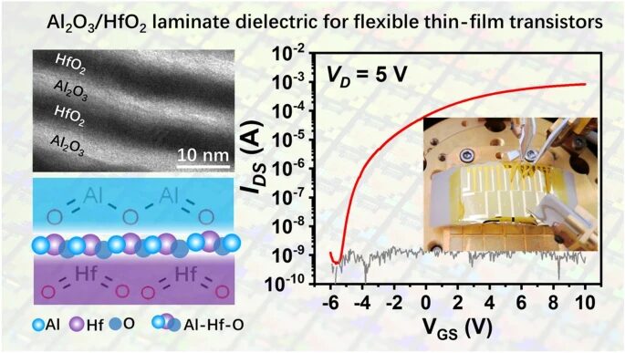
3. The carrier mobility of the flexible TFT is 9.7 cm²V⁻¹s⁻¹, with an on/off ratio of approximately 1.3 × 10⁶, a subthreshold voltage of 0.1 V, a saturation current of up to 0.83 mA, and a subthreshold swing of 0.256 Vdec⁻¹.
Content Summary
Illustrative Guide
In this study, all TFTs with a bottom-gate top-contact structure were fabricated using a typical photolithography process. Inspired by the ability of nanolaminate structures to produce high-density, moisture-resistant, and oxidation-resistant flexible films, a stacked Al₂O₃/HfO₂ insulating layer with varying numbers of layers was manufactured by controlling the processing steps of the ALD process. The specific preparation procedures and related parameters for each layer are shown in Figure 1(a). Figure 1(b) presents the optical microscopy image of the fabricated TFT device, from which the effective channel length of the device can be calculated to be 20 μm and the width is 100 μm. After peeling the polyimide (PI) substrate from the silicon wafer, the flexible PI-based TFT with a bending radius of 40 mm is shown in Figure 1(c).
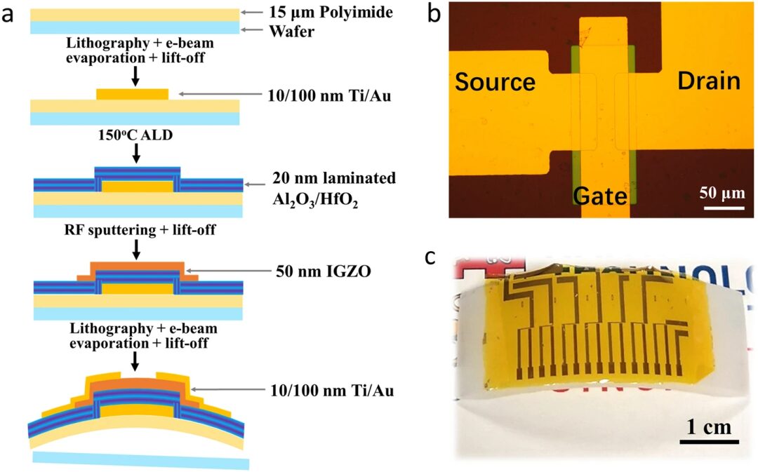
Figure 1. (a) Schematic diagram of the manufacturing process of IGZO-based TFT with a stacked Al₂O₃/HfO₂ insulating layer, including thickness information for each layer; (b) Microscopic image of the fabricated TFT device; (c) Photo of the TFT on a flexible substrate with an Al₂O₃/HfO₂ insulating layer.
II Electrical Performance Testing of IGZO-Based TFT with Stacked Al₂O₃/HfO₂ Insulating Layer
To demonstrate the performance of IGZO-based TFTs, the electrical performance of TFTs with different insulating layers deposited at 150°C was compared, as illustrated in Figure 2. Figures 2(a), (d), and (g) show the transfer characteristics of TFTs with stacked Al₂O₃/HfO₂, HfO₂, and Al₂O₃ insulating layers, respectively, where the maximum drain current of the stacked Al₂O₃/HfO₂ is as high as 0.7 mA, which is 350% and 260% higher than that of TFTs with HfO₂ and Al₂O₃ insulating layers, respectively. As shown in Figures 2(b), (e), and (h), the threshold voltages for the three insulating layer TFTs are 0.1 V, 2.1 V, and 1.7 V, respectively. Figures 2(c), (f), and (i) display the output characteristics of the TFTs with stacked Al₂O₃/HfO₂, HfO₂, and Al₂O₃ insulating layers, with an applied VGS range of 2-10 V and a step size of 2 V. From the figures, it can be seen that the saturation current and pinch-off regions of the three samples are clearly visible, indicating that VGS can effectively control the channel current. Additionally, the absence of current crowding effects in these three TFTs also indicates good contact between the source-drain and conductive channel. At a VGS of 10 V, the TFT with the stacked Al₂O₃/HfO₂ insulating layer has an IDS (0.42 mA) at least twice as large as that of the TFTs with HfO₂ (0.18 mA) and Al₂O₃ (0.13 mA) insulating layers, which can be attributed to the thermodynamic stability, high density, good corrosion resistance, and high saturation carrier mobility of the stacked Al₂O₃/HfO₂.
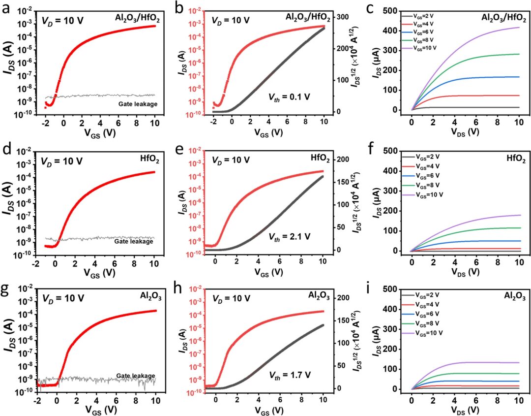
Figure 2. Transfer characteristics, IDS curves, and output characteristics of IGZO-based TFTs fabricated with different insulating layers: (a)-(c) stacked Al₂O₃/HfO₂; (d)-(f) HfO₂; (g)-(i) Al₂O₃.
III Morphological and Microstructural Characterization of Al₂O₃/HfO₂ Nanolaminate
To characterize the morphology and microstructure of the Al₂O₃/HfO₂ nanolaminate deposited at 150°C via ALD, cross-sectional TEM-EDS analysis of the IGZO/Al₂O₃/HfO₂ layers of the TFT device was performed. The SEM image of the sample prepared using a dual-beam FIB system is shown in Figure 3(a). Figure 3(b) displays the cross-sectional TEM image of the Al₂O₃/HfO₂ nanolaminate, where five layers with a total thickness of about 20 nm can be observed, consisting of light layers (Al₂O₃) and dark layers (HfO₂) with low interface roughness and good thickness uniformity. From the HRTEM in Figure 3(c), it can be seen that the Al₂O₃ layer is amorphous, while the lattice fringes of HfO₂ can be clearly observed, indicating its crystalline state. Additionally, the FFT diffraction pattern in Figure 3(d) also clearly demonstrates the single-crystal nature of the HfO₂ layer. As shown in Figure 3(e), the cross-sectional EDS mapping of IGZO/Al₂O₃/HfO₂ clearly shows the distribution of Zn, In, Ga, Al, Hf, C, and O elements. Figures 3(f–i) display the EDS maps of Hf, Al, In, and O elements, respectively.
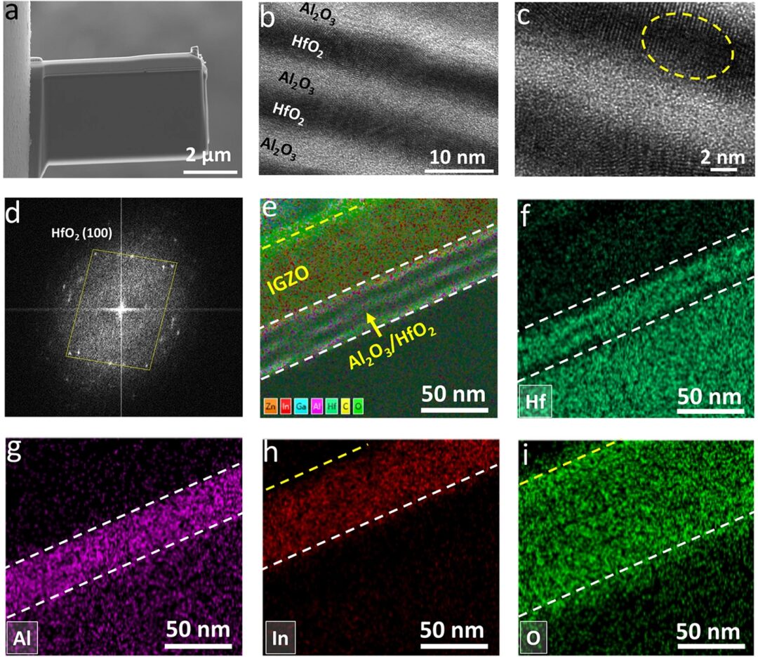
Figure 3. (a) SEM image of the TEM sample prepared by FIB; cross-section of the stacked Al₂O₃/HfO₂ insulating layer deposited at 150°C (b) TEM and (c) HRTEM; (d) FFT diffraction pattern obtained from the dashed region in (c); (e) Cross-sectional TEM-EDS elemental mapping of elements Zn, In, Ga, Al, Hf, C, and O; (f-i) EDS mapping of Hf, Al, In, and O.
IV Elemental Composition and Chemical Analysis of Al₂O₃/HfO₂ Nanolaminate
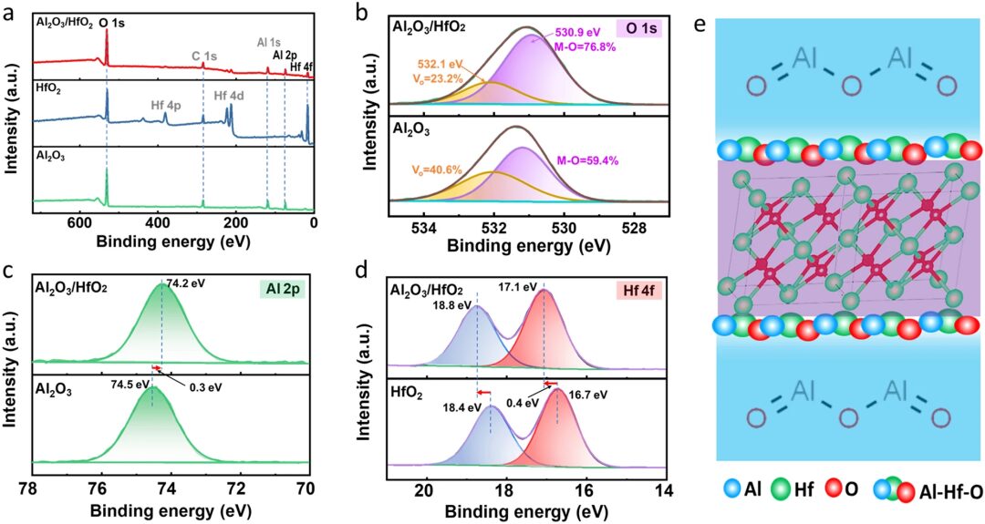
Figure 4. (a) X-ray photoelectron spectra of the fabricated stacked Al₂O₃/HfO₂, HfO₂, and Al₂O₃ insulating layers; high-resolution (b) O 1s and (c) Al 2p spectra of the stacked Al₂O₃/HfO₂ nanolaminate and Al₂O₃; (d) High-resolution Hf 4f spectra of the stacked Al₂O₃/HfO₂ and HfO₂; (e) Schematic diagram of the Al₂O₃/HfO₂ nanolaminate with amorphous Al₂O₃, crystalline HfO₂, and aluminum oxide (Al-Mg-O) phases at the interface.
V Bending Performance Testing of Flexible TFT with Stacked Al₂O₃/HfO₂ Insulating Layer
The flexible TFT on a PI substrate is made from the Al₂O₃/HfO₂ nanolaminate deposited at 150°C via ALD. As shown in Figure 5(a), the flexible TFT with Al₂O₃/HfO₂ nanolaminate can be tested on a curved surface with a bending radius of 40 mm. Figure 5(b) shows the transfer characteristics of the PI-based flexible TFT with a fixed VDS of 3 V. The leakage current of the device is in the range of 10-9 A, with a maximum Ion of up to 0.83 mA, achieving a switch current ratio greater than 106. From the intersection of IDS and VGS in Figure 5(c), the threshold voltage of 2.8 V can be extracted. Figure 5(d) shows the output characteristics, where VGS is increased from 2 V to 10 V in 2 V steps, and the output characteristic curve shows saturated IDS, with IDS reaching up to 0.72 mA at VGS of 10 V. Figure 5(e) shows the transfer characteristics of the flexible IGZO-based TFT after 100 cycles of repeated bending at a bending radius of 40 mm. Additionally, Figure 5(f) summarizes the stable maximum IDS and average gate leakage of the fabricated TFTs. These electrical performances of the IGZO-based flexible TFT demonstrate good flexibility and durability.
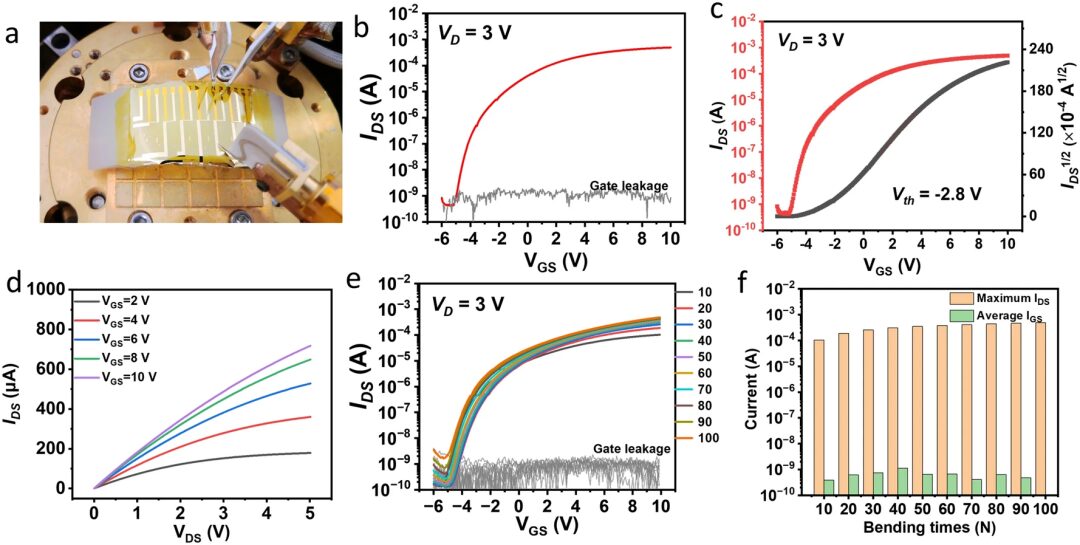
Figure 5. (a) Photo of the PI-based flexible TFT with Al₂O₃/HfO₂ nanolaminate tested on a curved surface with a bending radius of 40 mm; (b) Transfer characteristics of the flexible TFT tested at a bending radius of 40 mm, (c) IDS curve, and (d) output characteristics; (e) Transfer characteristics of the IGZO-based flexible TFT after 100 cycles of repeated bending at a bending radius of 40 mm, (f) maximum IDS and average IGS.
VI Humidity Stability and Yield of IGZO-Based TFT with Stacked Al₂O₃/HfO₂ Insulating Layer
The humidity stability and hysteresis characteristics of the fabricated IGZO-based TFT with stacked Al₂O₃/HfO₂ insulating layer were studied by storing the devices in a laboratory environment (relative humidity of 60-70%, temperature of 25-30°C) for different periods. As shown in Figure 6(a), the gate leakage of the IGZO-based TFT with stacked Al₂O₃/HfO₂ insulating layer remains stable at about 10-10 A. Meanwhile, after exposing the TFT to an environment with a relative humidity of 60–70% and a temperature of 25–30°C for 48 hours, it exhibits ideal transfer behavior with only minor hysteresis characteristics. In addition, the reliability of the IGZO-based TFT with stacked Al₂O₃/HfO₂ insulating layer was also investigated. As shown in Figure 6(b), a total of 49 IGZO-based TFT units were tested in 7 groups, with only two units in the 3rd and 4th groups being damaged, while the other 47 units worked well, with an average maximum IDS of 0.79 mV, achieving a yield of up to 95% for the IGZO-based TFT with stacked Al₂O₃/HfO₂ insulating layer.
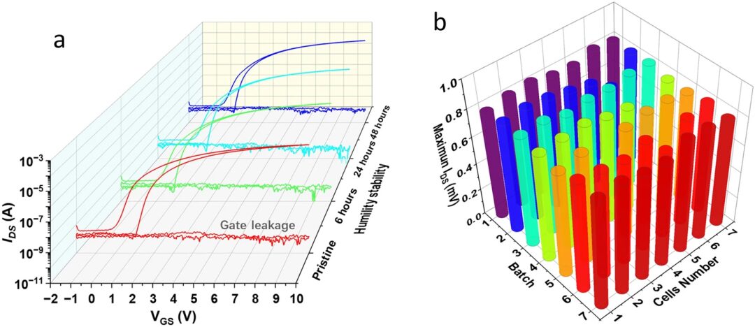
Figure 6. (a) Transfer characteristics and hysteresis characteristics of the flexible TFT with stacked Al₂O₃/HfO₂ insulating layer in its original state and after being stored for 6 h, 24 h, and 48 h in a laboratory environment (relative humidity of 60-70%, temperature of 25-30°C); (b) 3D bar chart showing the maximum IDS of IGZO-based TFTs in 7 groups (7 units per group).
Author Information

First author of this article

First author of this article

Corresponding author of this article
▍Main Research Achievements
▍Email:[email protected]
Link to the paper:
(Click the “Read the original” button in the lower-left corner to go directly to the original article)
Welcome to leave comments and share your views.Support the authors by clicking the “Like” and “Looking”↓↓↓