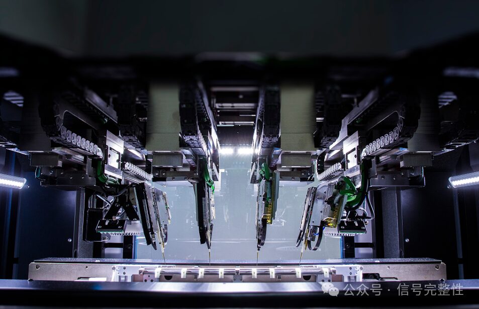
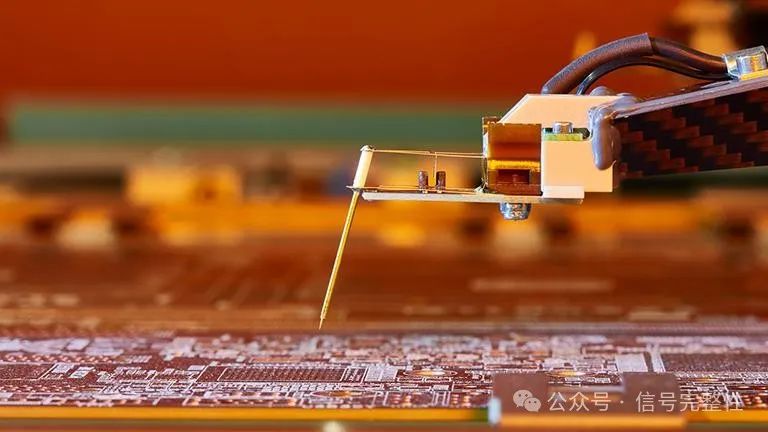
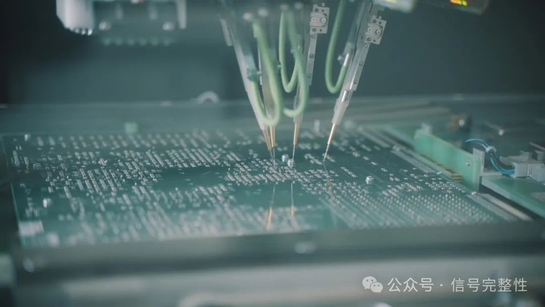
Flying probe testing is currently the best solution for some major issues in electrical testing. It uses probes to replace the test bed, employing multiple motor-driven electrical probes that can move quickly to contact the pins of the device for electrical measurements.

During the production process of PCB boards, it is inevitable that external factors may cause electrical defects such as short circuits, open circuits, and leakage. As PCB circuit boards continue to evolve towards high density, fine pitch, and multilayer designs, if defective boards are not screened out in a timely manner and allowed to flow into the manufacturing process, it will undoubtedly lead to greater cost waste. Therefore, in addition to improving process control, enhancing testing technology can also provide PCB manufacturers with solutions to reduce scrap rates and improve product yield.

Methods of electrical testing include: Dedicated, Universal Grid, Flying Probe, E-Beam, Conductive Fabric, Capacitive, and ATG-SCANMAN. Among these, three commonly used devices are the dedicated tester (automatic universal PCB tester), high-quality universal tester, and flying probe tester.
What are the differences between flying probe testing and test fixtures? What are their respective advantages?
Flying probe testing: This method utilizes 4 to 8 probes to perform high-voltage insulation and low-resistance continuity testing on the circuit board, testing for open and short circuits without the need for dedicated test fixtures. The PCB is directly placed into the flying probe tester, and the test program is run to perform the tests. The advantages of flying probe testing lie in its convenience in testing methods and operational processes, saving on testing costs, eliminating the time required to create test fixtures, and improving shipping efficiency, making it suitable for small batch production of PCBs.

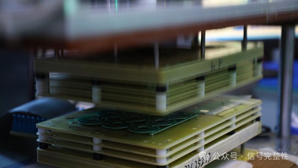
On the other hand, a test fixture is a specialized testing jig designed for continuity testing of mass-produced PCB boards, which has a higher manufacturing cost but better testing efficiency and does not incur charges for reorders.
In terms of the applicability of testing technology, flying probe testing is currently suitable for small batch and sample electrical testing equipment. However, when used for medium to large-scale production, the slow testing speed and high equipment costs will significantly increase testing costs. In contrast, both universal and dedicated types can achieve economies of scale for PCB boards of any level as long as the production quantity reaches a certain number, with testing costs typically accounting for only 2-4% of the selling price. This is why universal and dedicated types are the main types of testing machines for mass production.
Working principle of flying probe testing
The flying probe tester is an improvement over traditional bed-of-nails online automatic high-voltage PCB testers, replacing the test bed with probes.
During operation, the unit under test (UUT) is conveyed into the tester via a belt or other UUT transfer system, where the tester’s probes make contact with the test pads and vias to test individual components on the UUT. The test probes are connected to drivers and sensors via a multiplexing system to test the components on the UUT. When one component is being tested, other components on the UUT are electrically shielded by the probes to prevent reading interference.

The flying probe tester can check for short circuits, open circuits, and component values. A camera is also used in flying probe testing to help locate missing components, inspecting the shapes of components with defined orientations, such as polarized capacitors.
With the probe positioning accuracy and repeatability reaching a range of 5-15 micrometers, the flying probe tester can precisely detect the UUT. Flying probe testing addresses many existing issues seen in PCB assembly: such as the potential 4-6 week testing development cycle; the inability to economically test small batch productions; and the inability to quickly test prototype assemblies.
Flying probe testing is a method for checking the electrical functionality of PCB boards (open/short circuit testing). The flying probe tester is a system for testing PCB circuit boards in a manufacturing environment. Instead of using the traditional bed-of-nails interfaces found in traditional online testers, flying probe testing employs four to eight independently controlled probes that move to the components being tested. The unit under test (UUT) is conveyed into the tester via a belt or other UUT transfer system. The tester’s probes then contact the test pads and vias to test individual components on the UUT. The test probes are connected to drivers (signal generators, power supplies, etc.) and sensors (digital multimeters, frequency counters, etc.) via a multiplexing system to test the components on the UUT. When one component is being tested, other components on the UUT are electrically shielded by the probes to prevent reading interference.
1. Charge/Discharge Time Method
The charge/discharge time for each network (also known as net value) is fixed. If there are networks with equal values, they may be shorted, requiring only a short circuit measurement between networks with equal values. The testing steps are as follows: for the first board: full open circuit test → full short circuit test → network value learning; for subsequent boards: full open circuit test → network value test, and if a short circuit is suspected, use the resistance method for testing. The advantages of this testing method are accurate results and high reliability; however, the first board’s testing time is long, and the number of retests is high, resulting in low testing efficiency. The most representative machine is MANIA’s SPEEDY machine.
2. Inductance Measurement Method
The principle of the inductance measurement method is to use one or several large networks (generally ground networks) as antennas, applying a signal to them, causing other networks to induce a certain inductance. The tester measures the inductance of each network, comparing the inductance values; if the inductance values are the same, there may be a short circuit, followed by short circuit testing. This testing method is only suitable for boards with ground layers; testing reliability is low for double-sided boards (without ground networks); when there are multiple large-scale networks, since more than one probe is used to apply the signal, the number of probes available for testing decreases, resulting in low testing efficiency. The advantages are high testing reliability and low retest rates. The most representative machines are ATG’s A2 and A3 models, which are equipped with 8 and 16 probes to improve testing efficiency.
3. Capacitive Measurement Method
This method is similar to the charge/discharge time method. According to the relationship between conductive patterns and capacitance, if a reference plane is set, with the distance from the conductive pattern to it being L, and the area of the conductive pattern being A, then C=εA/L. If an open circuit occurs, the area of the conductive pattern decreases, and the corresponding capacitance decreases, indicating an open circuit; if two conductive patterns are connected, the capacitance response increases, indicating a short circuit. In open circuit testing, the capacitance values at the endpoints of the same network should be equal; if they are not, an open circuit exists, and the capacitance values of each network should be recorded for comparison during short circuit testing. The advantages of this method are high testing efficiency, while the downside is that it relies entirely on capacitance, which can be influenced by many factors, resulting in lower testing reliability compared to the resistance method, especially due to measurement errors caused by associated capacitance and secondary capacitance. Testing reliability is lower for networks with fewer endpoints (such as single-point networks). Currently, flying probe testers using this method include those from HIOKI and NIDEC READ.
4. Phase Difference Method
This method involves applying a sine wave signal to the ground or electrical layer, obtaining the phase lag angle from the line layer to derive capacitance or inductance values. The testing steps are: for the first board, test open circuits first, then measure the phase difference values of other networks, and finally test for short circuits; for subsequent boards, test open circuits, then measure network phase difference values, and use the resistance method for verification of suspected short circuits. The advantages are high testing efficiency and reliability; however, it is only suitable for testing boards with four or more layers; for double-sided boards, the resistance method must be used. Companies currently using this testing method include MicroCraft.
5. Adaptive Testing Method
The adaptive testing method allows the device to select an appropriate testing process based on the specific conditions and testing specifications after each testing application is completed. For example, if the network value (charging time or capacitance, etc.) of a network is less than the device’s testing error, the device will automatically adopt resistance testing and electric field testing. This testing method is the fastest and provides the best testing results. However, there are currently no testers known to use this method.
The flying probe tester is an improvement over traditional bed-of-nails testers, using probes instead of a test bed. It is equipped with four heads, each with two test probes that can move independently at high speed, with a minimum testing gap of 0.2 mm. During operation, the unit under test (UUT) is conveyed into the tester via a belt or other UUT transfer system, where the tester’s probes make contact with the test pads and vias to test individual components on the UUT. The test probes are connected to drivers (signal generators, power supplies, etc.) and sensors (digital multimeters, frequency counters, etc.) via a multiplexing system to test the components on the UUT. When one component is being tested, other components on the UUT are electrically shielded by the probes to prevent reading interference.
The flying probe tester can check for short circuits, open circuits, and component values. A camera is also used in flying probe testing to help locate missing components, inspecting the shapes of components with defined orientations, such as polarized capacitors. With the probe positioning accuracy and repeatability reaching a range of 5-15 micrometers, the flying probe tester can precisely detect the UUT.
I have improved my understanding of PCB design through various processes【1】Driven by interest and passion
I have improved my understanding of PCB design through various processes【2】Should hardware engineers design PCBs themselves?
I have improved my understanding of PCB design through various processes【3】How long should PCB traces be??
I have improved my understanding of PCB design through various processes【4】How wide should PCB traces be?
I have improved my understanding of PCB design through various processes【5】Inner layers of PCB
I have improved my understanding of PCB design through various processes【6】 vias
I have improved my understanding of PCB design through various processes【7】Can PCBs use sharp angles and right angles?
I have improved my understanding of PCB design through various processes【8】Should copper islands be retained? (PCB islands)
I have improved my understanding of PCB design through various processes【9】Can vias be placed on pads??
I have improved my understanding of PCB design through various processes【10】What materials are PCBs made of, what is FR4?
I have improved my understanding of PCB design through various processes【11】Why is the solder mask mostly green?
I have improved my understanding of PCB design through various processes【12】Stencil
I have improved my understanding of PCB design through various processes【13】Pre-layout
I have improved my understanding of PCB design through various processes【14】Principles of PCB layout and routing
I have improved my understanding of PCB design through various processes【15】Cross-segment routing
I have improved my understanding of PCB design through various processes【16】Signal reflection
I have improved my understanding of PCB design through various processes【17】Dirty signals
I have improved my understanding of PCB design through various processes【18】Surface treatment processes such as immersion gold, gold plating, and tin spraying
I have improved my understanding of PCB design through various processes【19】Trace spacing
I have improved my understanding of PCB design through various processes【20】Placement of capacitors
I have improved my understanding of PCB design through various processes【21】Crosstalk