Source: Semiconductor Materials and Process Equipment
Original Author: XKX
This article aims to analyze the core elements of the semiconductor field, starting from the most basic crystal structure and gradually delving into the applications of semiconductors in integrated circuits.
In our daily lives, semiconductors are everywhere. From smartphones to televisions, from cars to microwaves, and even the medical devices we use, the shadow of semiconductors is behind all modern technology. However, despite the widespread applications of semiconductors, the concepts and working principles of semiconductors remain unfamiliar to most people.
The development of semiconductors has led to a technological revolution, from early transistor radios to modern large-scale integrated circuits, the advancements in semiconductors have driven the entire information age. However, semiconductors are not just the driving force of technology; they are also an important window for us to understand the world. By studying semiconductors in depth, we can better understand the behavior of materials and how we can use this knowledge to create technologies that change the world.
In this article, we will first analyze the basic concepts of semiconductors, then explore their crystal structures and how these structures affect their properties. Next, we will introduce some commonly used semiconductor materials and their applications in electronic devices. Then, we will delve into the role of semiconductors in integrated circuits and how these integrated circuits have become the core of modern electronic devices. Finally, we will look ahead to the future development of semiconductor technology and the impact this development will have on our lives.
Basic Concepts of Semiconductors
First, we need to understand what a semiconductor is. A semiconductor is a material whose electrical properties lie between those of conductors and insulators. Its electrical conductivity is low at room temperature but can significantly increase with rising temperature or changes in external conditions such as light exposure. This characteristic makes semiconductors valuable in electronic devices.
To understand semiconductors in depth, we need to introduce some physical concepts, such as energy bands, forbidden bands, and charge carriers. In solid materials, the energy states of electrons form a series of energy levels, and closely spaced energy levels form energy bands. In semiconductors, the electron energy levels form two main energy bands: the valence band and the conduction band. The electrons in the valence band belong to the inherent electrons of the atoms and are usually bound close to the atoms; while the electrons in the conduction band have higher energy and can move freely, thus conducting electricity.
The region between the two energy bands is called the forbidden band, which is an energy level region without electrons. In semiconductors, the width of the forbidden band is moderate, allowing some electrons to jump from the valence band to the conduction band by absorbing thermal or optical energy, forming free electrons and holes. These two types of particles are collectively referred to as charge carriers, which can move under the influence of an electric field, thus forming an electric current.
Through these basic physical concepts, we can better understand the working principles of semiconductors. In the following sections, we will delve into the crystal structures of semiconductors and how these structures affect their electrical properties.
Crystal Structures and Semiconductors
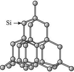
The properties and performance of semiconductors largely depend on their crystal structures. The crystal structure refers to the arrangement of atoms in solid materials, which has a significant impact on the physical and chemical properties of the material. Let’s take a look at the two most common elements in semiconductors: silicon and germanium.
Both silicon and germanium belong to group IVA of the periodic table, and they both have four outer shell electrons, making their arrangement in the crystal very similar. In the crystal structures of silicon and germanium, each atom forms covalent bonds with four surrounding atoms, resulting in a crystal structure known as diamond structure.
This diamond structure gives semiconductors several important properties. First, the formation of covalent bonds imparts high mechanical strength and chemical stability to the crystal. Secondly, since the electrons in the valence band are bound in covalent bonds, the electrical conductivity of semiconductors is low at room temperature. However, due to the moderate width of the forbidden band, some electrons can jump to the conduction band by absorbing thermal or optical energy, forming free electrons and holes, thus allowing semiconductors to have tunable electrical conductivity.
Additionally, the crystal structure of semiconductors also allows for doping. Doping refers to the introduction of small amounts of trivalent or pentavalent elements into semiconductors to alter their electrical properties. In the diamond structure of silicon or germanium, each atom has four covalent bonds, so introducing trivalent or pentavalent elements can create extra holes or free electrons, thereby changing the conductivity of the semiconductor.
By understanding the crystal structures of semiconductors, we can gain deeper insights into their unique electrical properties and working principles. In the following sections, we will explore more semiconductor materials and their applications in electronic devices.
The selection of semiconductors is broad, ranging from single elements like silicon and germanium to compound materials like gallium nitride or gallium arsenide, each with its unique properties and specific applications.
Silicon is the most commonly used semiconductor material, abundantly found in the earth’s crust and easy to extract and process. Silicon’s moderate forbidden band width gives it good semiconductor properties at room temperature. Moreover, silicon can form stable oxides, which are crucial for manufacturing metal-oxide-semiconductor (MOS) integrated circuits.
However, silicon is not a panacea. For some special applications, such as optoelectronic devices or high-frequency electronic devices, other types of semiconductors are typically chosen. For example, gallium arsenide has higher electron mobility, making it advantageous in high-speed electronic devices. On the other hand, gallium nitride is widely used in blue light-emitting diodes and power electronic devices due to its wide forbidden band and strong light emission performance.
Doping is an important tool for altering semiconductor properties. By introducing small amounts of dopant elements into semiconductors, we can change the type of conductivity, forming n-type or p-type semiconductors. In n-type semiconductors, pentavalent elements such as phosphorus or arsenic are added to silicon, creating extra free electrons. In p-type semiconductors, trivalent elements such as boron are added to silicon, creating extra holes.
Doping not only changes the conductivity of semiconductors but also enables the manufacture of complex semiconductor devices such as diodes and transistors. By controlling the type and concentration of dopants, we can form complex electrical structures in semiconductors, allowing for precise control of current.
In the following sections, we will delve deeper into the working principles of semiconductor devices and their applications in integrated circuits.
Semiconductors in Integrated Circuits
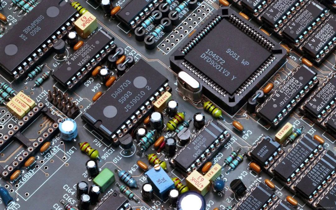
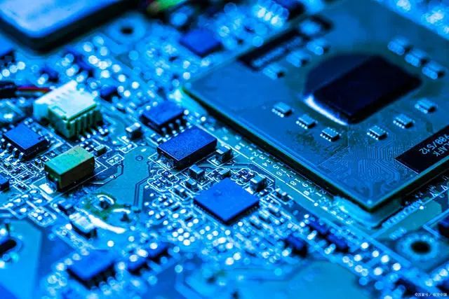
Having understood the basic concepts, crystal structures, and materials of semiconductors, we now explore the applications of semiconductors in integrated circuits. Integrated circuits, also known as microchips, are the core components of modern electronic devices. They consist of numerous miniature semiconductor devices, such as diodes, transistors, and capacitors, all integrated onto a small silicon chip.
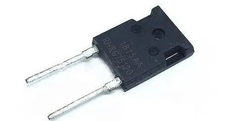
Transistors are the most important components of integrated circuits. They are three-terminal devices composed of a source, drain, and gate. The working principle of transistors is based on the behavior of charge carriers in semiconductors. The p-n junction formed between n-type and p-type semiconductors can control the flow of current. By controlling the number of charge carriers through changing the gate voltage, we can control the current flowing from the source to the drain. This ability makes transistors the core switching elements in electronic devices.
The manufacturing of integrated circuits is a highly complex technology that involves many intricate process steps, such as oxidation, photolithography, etching, doping, and metallization. In this process, silicon wafers are built up layer by layer to form three-dimensional electronic device structures. With the advancement of process technology, we can now integrate billions of transistors on a single silicon chip, creating extremely complex electronic systems, such as microprocessors and memory.
The development of integrated circuits has ushered in the information age. It has made electronic devices smaller, cheaper, and more powerful, thus changing the way we live. In the following sections, we will look ahead to the future of semiconductor technology and the impact this development will have on our lives.
With the continuous development of technology, semiconductor technology is also advancing. On one hand, we are continuously improving the performance of electronic devices by increasing the integration of transistors. On the other hand, we are exploring new semiconductor materials and device structures to develop new types of electronic and optoelectronic devices.
In transistor technology, Moore’s Law predicts the ongoing reduction in transistor size and increase in integration. However, as transistor sizes approach atomic scales, we face many new challenges, such as quantum effects, thermal management, and process complexity. To overcome these challenges, researchers are exploring various new device structures and process technologies, such as multi-gate transistors, 3D integration, and new materials.
In terms of new materials, we are exploring various new semiconductor materials, such as two-dimensional materials, organic semiconductors, and high-temperature superconductors. These new materials possess unique electrical and optical properties, offering possibilities for developing new types of electronic and optoelectronic devices.
In optoelectronic devices, with the integration of optoelectronics and microelectronics, we are developing various new optoelectronic devices, such as lasers, optical modulators, and photodetectors. These devices have broad application prospects in communication, information processing, and sensing fields.
The future of semiconductor technology is full of challenges and opportunities. We look forward to more technological breakthroughs to drive our social progress.
END
Reprinted content represents the author’s views only
Does not represent the position of the Semiconductor Institute of the Chinese Academy of Sciences
Editor: March
Responsible Editor: Six Dollar Fish
Submission Email: [email protected]
1. The Semiconductor Institute has made progress in the research of bionic coverage neuron models and learning methods
2. The Semiconductor Institute has made significant progress in the inverted structure perovskite solar cells
3. Why is copper used as the interconnect metal for chips?
4. What exactly is 7nm in chips
5. Silicon-based integrated photonic quantum chip technology
6. How abnormal is the quantum anomalous Hall effect? It may bring about the next revolution in information technology!