Source: Semiconductor Materials and Technology Equipment
Original Author: XKX
Early Semiconductor Technology
1.1 The Birth of Diodes and Transistors
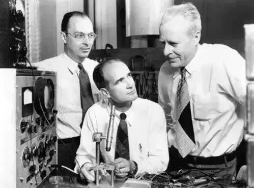
The birth of the transistor is considered a major breakthrough in the history of semiconductor technology. In 1947, William Shockley and Walter Brattain at Bell Labs successfully created the first solid-state transistor. The transistor is a semiconductor device that can amplify electrical signals, replacing the large and fragile vacuum tubes used at the time. This invention ushered in an era of miniaturization and performance enhancement in electronic devices, paving the way for the rapid development of computer and communication technologies.
1.2 The First Application of Silicon Materials
In the early stages of semiconductor technology, silicon was first used to manufacture semiconductor devices. Silicon is one of the most abundant materials in the Earth’s crust and has good electronic properties, such as stability and controllability. In 1954, German physicist Karl Heinrich Daimler successfully prepared silicon single crystals, providing high-quality semiconductor materials for the manufacturing of semiconductor devices.
Silicon has shown excellent performance in the manufacture of transistors and other semiconductor devices due to its stable electronic properties and ability to operate at high temperatures. This discovery marked the emergence of silicon materials in the semiconductor industry and laid a solid foundation for subsequent integrated circuit manufacturing.
1.3 Foundations of Transistor Manufacturing Processes
Early transistor manufacturing processes involved precise manual operations, including manual cutting of silicon wafers and manual installation of electrode wires. However, this manufacturing method was costly and inefficient.
In the late 1950s, the introduction of Moore’s Law inspired scientists and engineers to continuously seek ways to improve the efficiency of transistor manufacturing. They gradually introduced automated manufacturing technologies, such as photolithography, thin-film deposition, and chemical etching, to accelerate the mass production of transistors. The introduction of these processes made transistors more reliable, cheaper, and higher performing, laying the foundation for the booming development of the semiconductor industry.
In summary, the early development of semiconductor technology was based on the invention of diodes and transistors, which fundamentally changed the performance and availability of electronic devices. At the same time, the first application of silicon materials and the introduction of automated manufacturing technologies also laid a solid foundation for the further evolution of semiconductor technology. These milestones paved the way for continuous advancements in semiconductor technology, impacting various aspects of modern society.
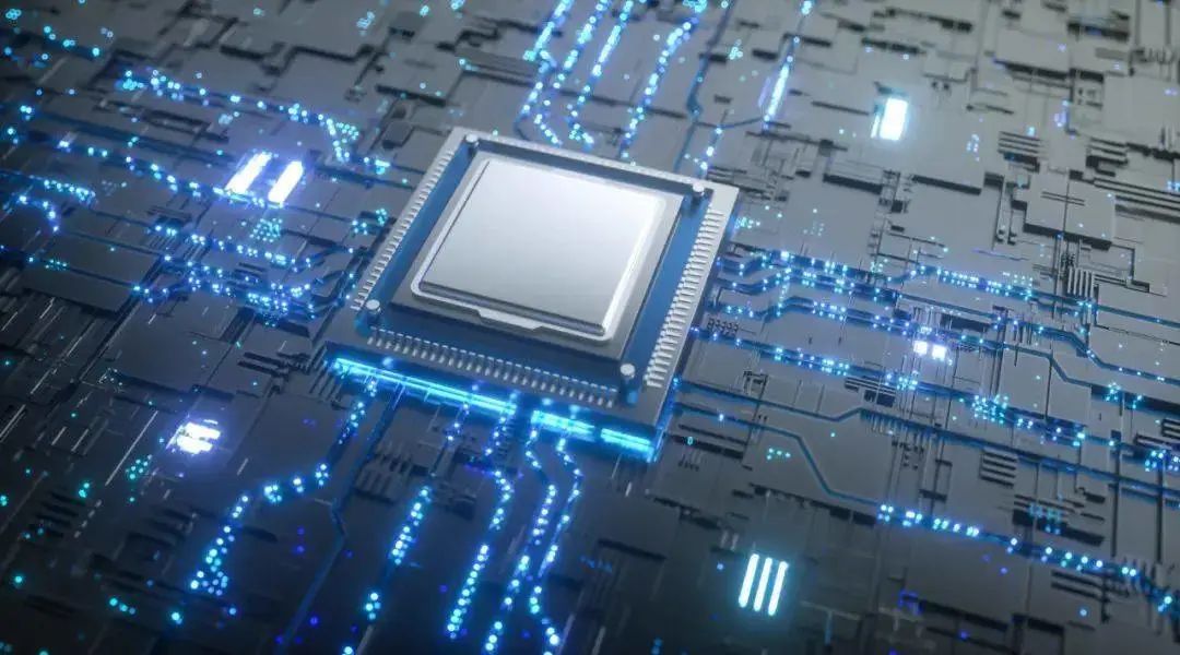
The Rise of Integrated Circuits
2.1 The Birth of the First Integrated Circuit

The Miniaturization of Semiconductor Technology
3.1 The Emergence of Advanced Manufacturing Technologies
In response to the challenges of nanoscale manufacturing, engineers and scientists have developed a series of advanced manufacturing technologies, which have made the manufacturing of semiconductor devices at the nanoscale possible, driving continuous advancements in semiconductor technology. These include:
-
Nano-lithography technology: Using extreme ultraviolet (EUV) and other high-energy light sources to create nanoscale patterns. EUV lithography machines can achieve higher resolutions than traditional UV lithography, aiding in the manufacture of ultra-small devices.
-
High-resolution electron beam exposure: Using electron beams to create extremely small patterns, with precise control capabilities making it a key technology in micro-nano manufacturing.
-
Chemical mechanical polishing: Used to flatten silicon wafer surfaces to ensure manufacturing precision at small sizes.
-
High-resolution thin-film deposition and etching technologies: Used to deposit ultra-thin layers of material on chips or remove unnecessary materials.
3.2 The Development of 3D Integrated Circuits
As transistor sizes continue to shrink, engineers have begun to explore vertical integrated circuits, or 3D integrated circuits, to further enhance the performance of integrated circuits. In traditional planar integrated circuits, components are located on the same plane, while in 3D integrated circuits, components can be stacked in multiple vertical layers. This structure allows for more transistors and components to be stacked on the same chip, increasing integration.
The manufacture of 3D integrated circuits involves complex challenges such as stacking multiple silicon wafers, high-density through-silicon vias, and cooling solutions. However, the development of this technology is expected to further enhance the performance of integrated circuits, reduce circuit board sizes, lower power consumption, and provide more possibilities for future high-performance computing and mobile devices.
In summary, the miniaturization of semiconductor technology is one of the key driving forces behind the continuous advancement of the semiconductor industry. Overcoming the challenges of nanoscale manufacturing and introducing advanced manufacturing technologies, such as nano-lithography and 3D integrated circuits, have had a profound impact on the evolution of the semiconductor industry. These innovations have driven improvements in integrated circuit performance, allowing us to enjoy smaller and higher-performing electronic devices while providing a solid foundation for future technological advancements.
Advancements in Materials Science
4.1 The Emergence of New Semiconductor Materials
-
Gallium Arsenide (GaAs): Gallium arsenide is a III-V semiconductor material with high electron mobility and high saturation velocity. This makes it perform excellently in high-frequency and high-speed applications, such as radar systems and communication devices.
-
Silicon Carbide (SiC): Silicon carbide is a wide-bandgap semiconductor material with good high-temperature and high-voltage characteristics. It is widely used in power electronic devices, electric vehicles, solar inverters, and other high-power applications.
-
Gallium Nitride (GaN): Gallium nitride is a wide-bandgap semiconductor material with high electron mobility and high saturation velocity, suitable for RF power amplifiers, LED lighting, and power electronics.
-
High-frequency electronic devices: Gallium arsenide is widely used in high-frequency communication, radar systems, and satellite communication to manufacture high-frequency power amplifiers and microwave components. Its high electron mobility allows it to perform excellently in high-frequency applications.
-
High-temperature and high-voltage electronic devices: The thermal stability and high-voltage characteristics of silicon carbide make it very suitable for applications in high-temperature environments or those requiring high-voltage operations, such as electric vehicles, power electronics, and high-temperature electronic devices.
-
High-efficiency optoelectronic devices: Gallium nitride is widely used in high-brightness LED lighting, blue laser diodes, solar cells, and UV detectors, replacing traditional silicon materials.
Future Prospects
Quantum computing is a highly anticipated field that utilizes the superposition and quantum entanglement of qubits to provide unprecedented computing power for solving complex problems and cracking encryption algorithms. In the development of quantum computing, quantum semiconductors will play a key role, as they can provide stable qubits and the foundational building blocks for quantum gates.The prospects of quantum semiconductors include:
-
Greater computational power: Quantum computing is expected to achieve significant breakthroughs in solving problems that are currently unsolvable, such as materials science, drug design, and climate simulation.
-
Communication security: Quantum semiconductors can also be used to build quantum communication systems that have super security, suitable for encrypting and decrypting communications.
-
New sensor technologies: Quantum semiconductors can also be used to manufacture highly sensitive sensors for detecting minute physical and chemical changes, which are significant in fields such as medicine and the environment.
5.2 Flexible Electronics and Wearable Technology
Flexible electronics and wearable technology are changing the way we interact with electronic devices. These technologies utilize flexible semiconductor materials, allowing devices to better conform to the shape and movement of the human body while maintaining excellent performance. Future prospects include:
-
Wearable health monitoring devices: Flexible electronics can produce more comfortable and skin-conforming health monitoring devices for real-time monitoring of vital signs and disease tracking.
-
Flexible displays: Bendable and rollable flexible displays will change the form of traditional screens, creating new user interfaces and applications, such as wearable devices and foldable smartphones.
-
Smart textiles: Flexible electronics can be integrated into textiles to create smart clothing and smart textiles for monitoring movement, regulating temperature, and providing wearable electronic services.
5.3 The Potential for Biomedical Applications
The potential of semiconductor technology for biomedical applications is immense. The combination of micro-nano manufacturing and biosensing technology enables the development of a new generation of biomedical devices and treatment methods, with future prospects including:
-
Personalized medicine: Semiconductor chips can be used for rapid and precise gene sequencing and analysis, providing data support for personalized medicine to better predict, diagnose, and treat diseases.
-
Biosensors: Miniature biosensors can monitor biomarkers, cellular activities, and physiological changes within the body, aiding in early disease detection and treatment.
-
Miniaturization of medical devices: Micro-nano manufacturing technology allows medical devices to become smaller and more portable, such as portable medical diagnostic devices and implantable medical instruments.
In summary, future prospects include breakthroughs in quantum computing, the popularization of flexible electronics and wearable technology, and the widespread application of semiconductor technology in biomedical applications. Innovations in these fields will further drive technological advancement, improve our quality of life, provide new solutions to global challenges, and continue to change the landscape of semiconductor technology. Semiconductor technology will play a key role in the future technological revolution, driving the continuous development and progress of society.
Conclusion
The evolution of semiconductor technology has profoundly impacted modern technology over the past few decades, benefiting nearly every field from computing to communication, from medicine to entertainment. Semiconductor devices have become an indispensable part of modern society. The importance of semiconductor technology is reflected in several aspects:
-
The explosion of computational power: Advances in semiconductor technology have driven continuous increases in computational power, enabling modern computers to perform complex tasks, process massive amounts of data, and drive developments in artificial intelligence and machine learning.
-
The revolution in communication and the internet: The miniaturization and high performance of semiconductor devices have made high-speed broadband communication and the proliferation of the internet possible, changing the way people live and work.
-
Advancements in healthcare and life sciences: The application of semiconductor technology in medical diagnostics, gene sequencing, biosensing, and medical imaging is expected to improve healthcare and enhance the quality of life for patients.
-
A catalyst for emerging technologies: Semiconductor technology continues to drive the development of emerging technologies, such as quantum computing, flexible electronics, wearable technology, and biomedical applications, which have enormous innovation potential.
Despite the tremendous success of semiconductor technology over the past few decades, it also faces future challenges in physical dimensions and environmental sustainability. These challenges also come with opportunities, as the semiconductor industry has the chance to create new technologies and innovations in addressing these issues, further driving technological advancement. In summary, the future of semiconductor technology is filled with challenges and opportunities. As technology continues to evolve and innovate, the semiconductor industry will play an important role in driving technological progress, improving human life, and addressing global challenges. The development of this field will impact our future, providing us with more opportunities and possibilities.
END
The reproduced content only represents the author’s views
It does not represent the position of the Institute of Semiconductor, Chinese Academy of Sciences
Editor: March
Chief Editor: Muxin
Submission Email: [email protected]
1. The Institute of Semiconductor has made progress in research on bionic covering neuron models and learning methods.
2. The Institute of Semiconductor has made important progress in inverted structure perovskite solar cells.
3. Why is copper used as interconnect metal in chips?
4. What exactly is 7nm in chips?
5. Silicon-based integrated optical quantum chip technology.
6. How anomalous is the quantum anomalous Hall effect? It may bring the next information technology revolution!