This article introduces the origin of semiconductors, what semiconductors are, and the classification of semiconductors.
1. The Origin of Semiconductors
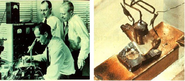
In January 1946, a semiconductor research group was officially established at Bell Labs in the United States, located across the Pacific. The group had three core members: Schokley, Bardeen, and Brattain, commonly known as the “Transistor Trio”.
The trio had their own research advantages; Bardeen proposed the surface state theory, Schokley provided the basic ideas for amplifiers, and Brattain designed the experiments.
In the following year, 1947, Bardeen and Brattain invented the point-contact transistor. In 1949, Schokley published a classic paper on p-n junctions and bipolar transistors. In the first transistor ever made, the two point contacts at the bottom of a triangular quartz crystal were created by pressing gold foil wires spaced 50μm apart onto the semiconductor surface, using germanium as the semiconductor material. When one contact was forward biased (i.e., positive voltage applied to the third terminal), and the other contact was reverse biased, the transistor action of amplifying the input signal could be observed.
Bipolar transistors are a key semiconductor device that ushered humanity into the modern electronic era, initiating the world-shaking semiconductor revolution…
At this point, a new term emerged – transistor.
We often hear another term – integrated circuit【Integrated Circuit: IC】. What is the relationship between transistors and integrated circuits?
Integrated circuits are made by integrating transistors, diodes, and other active devices along with passive components like resistors and capacitors on a single semiconductor chip through a series of specific planar manufacturing processes, encapsulated in a protective shell, and capable of performing specific functions in complex electronic systems.
Transistors are the building blocks of integrated circuits, and their invention accelerated the development of the semiconductor industry.
2. What Are Semiconductors?
The concept of semiconductors is described based on the conductivity of materials. In nature, all objects can be classified into three categories based on their conductivity: conductors, semiconductors, and insulators.
In our daily lives, we encounter objects that either conduct electricity, do not conduct electricity, or conduct electricity under specific conditions.
From the perspective of resistance, this can be illustrated in the following diagram:
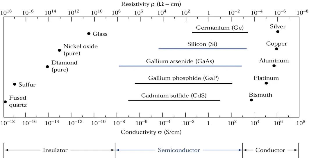
Insulators: Have very low conductivity, approximately between 20E-18S/cm to 10E-8S/cm, such as fused quartz and glass;
Conductors: Have relatively high conductivity, ranging from 10E4S/cm to 10E6S/cm, such as metals like aluminum and silver;
Semiconductors: Have conductivity that lies between insulators and conductors.
Why has this material with unstable conductivity received widespread attention and application?
Because semiconductors are easily affected by temperature, light, magnetic fields, and minute impurities.
Under external stimuli, the properties of semiconductor materials change, and it is this high sensitivity of conductivity that makes semiconductors one of the most important materials in various electronic applications.
3. Classification of Semiconductors
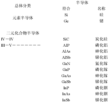
Semiconductors can be classified based on the type of materials:
(1) Elemental Semiconductors: Silicon (Si), Germanium (Ge)
Silicon and germanium are elemental semiconductors composed of single atoms, both belonging to Group IV of the periodic table.
In the early 1950s, germanium was the primary semiconductor material; however, after the early 1960s, silicon replaced germanium as the main material for semiconductor manufacturing, primarily because silicon devices exhibit better characteristics at room temperature, high-quality silicon oxide layers can be produced through thermal growth, and silicon is abundant, constituting 25% of the Earth’s crust, second only to oxygen.
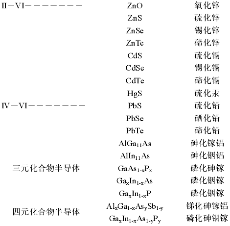
(2) Compound Semiconductors: Gallium Arsenide (GaAs), Indium Phosphide (InP), etc.
Compound semiconductors can be further subdivided based on the number of constituent elements:
(a) Binary Compound Semiconductors:
Composed of two elements, such as common examples:
IV-IV Group Element Compound Semiconductors: Silicon Carbide (SiC);
III-V Group Element Compound Semiconductors: Gallium Arsenide (GaAs), Gallium Phosphide (GaP), Indium Phosphide (InP), etc.;
II-VI Group Element Compound Semiconductors: Zinc Oxide (ZnO), Zinc Sulfide (ZnS), Cadmium Telluride (CdTe), etc.;
IV-VI Group Element Compound Semiconductors: Lead Sulfide (PbS), Lead Selenide (PbSe), Lead Telluride (PbTe)
(b) Ternary Compound Semiconductors, composed of three elements, such as:
Alloy semiconductors AlxGa(1-x)As composed of III Group element Aluminum (Al), Gallium (Ga), and V Group element Arsenic (As).
(c) Quaternary Compound Semiconductors: Composed of three or more elements.
Quaternary compound semiconductors of the form AxB(1-x)CyD(1-y) can be composed of many binary and ternary compound semiconductors. For example, the quaternary compound GaxIn(1-x)AsyP(1-y) alloy semiconductor is composed of Gallium Phosphide (GaP), Indium Phosphide (InP), and Gallium Arsenide (GaAs).
The classification of semiconductors is shown in the diagram below:
4. Why Can Silicon Be Used as a Semiconductor Material?
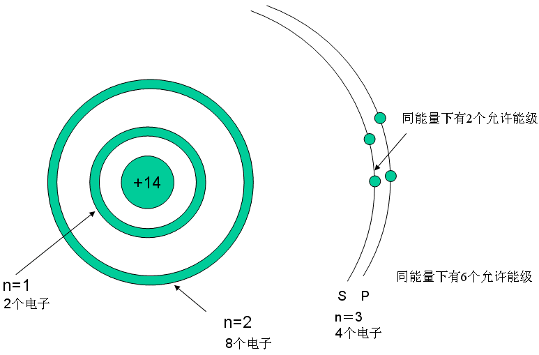
Silicon is located at position 14 in the periodic table, with 14 electrons in its outer shell. The diagram below shows the silicon crystal structure and its electron arrangement. Each silicon atom has four electrons in its outer shell, sharing four pairs of electrons with four surrounding atoms. This structure of shared electron pairs is called covalent bonding.
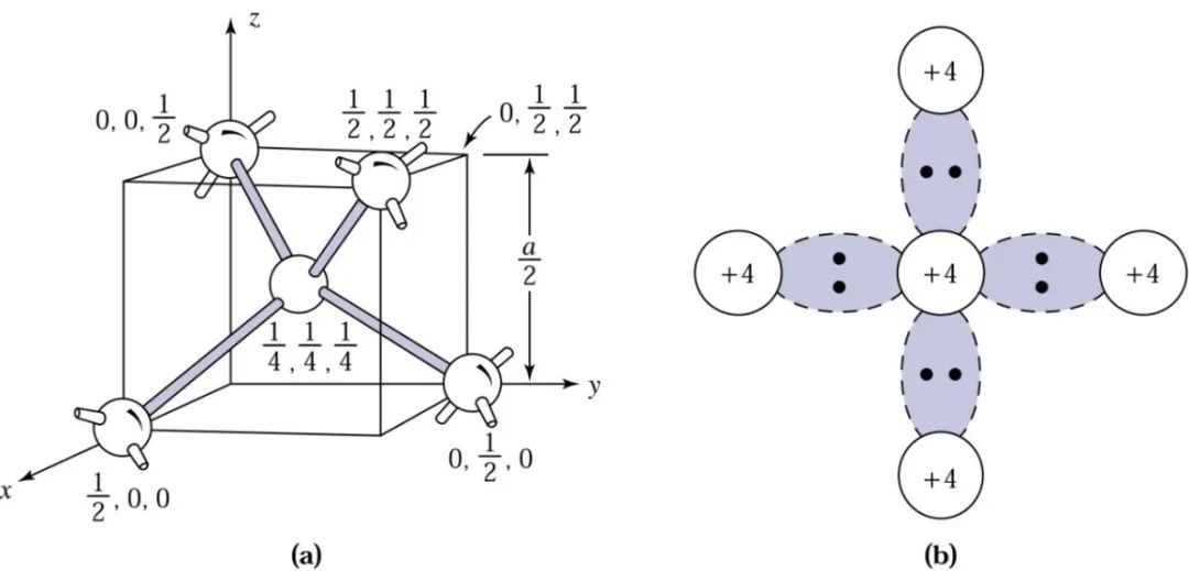
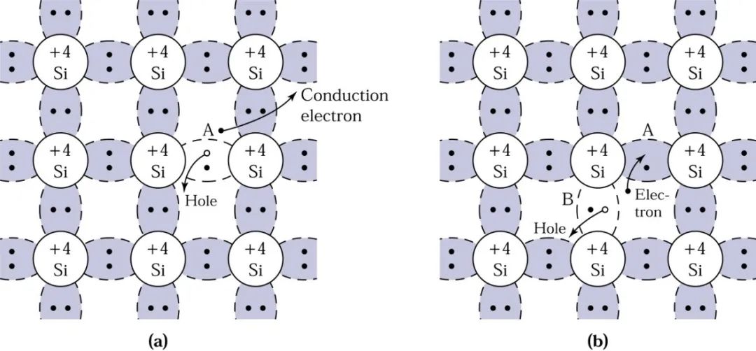
At low temperatures, electrons are bound in the tetrahedral lattice, making electrical conduction impossible. However, at high temperatures, thermal vibrations can break covalent bonds. When some bonds are broken, the free electrons generated can participate in electrical conduction. When a free electron is generated, it creates a vacancy where it was, which can be filled by a neighboring electron, resulting in the movement of the vacancy, which can be viewed as a positive charge moving in the opposite direction of the electron, called a hole. The mobile electrons and holes in semiconductors are collectively referred to as carriers.
The diagram below shows the process of hole movement:
As previously mentioned, elemental silicon has four electrons in its outer shell, and there is an additional detail to note: these four electrons are distributed over two orbits, similar to satellites orbiting the Earth, where four satellites orbiting in two spatial orbits around the Earth.
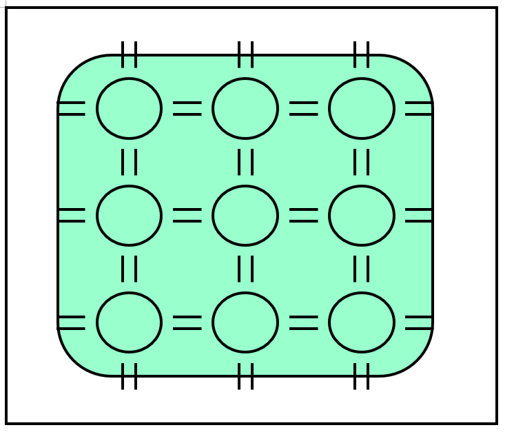
We know that semiconductor wafers are made of silicon, where silicon atoms are arranged in an orderly manner according to crystal production methods. From a planar perspective, the arrangement of silicon atoms is as follows:
From a three-dimensional perspective, the arrangement of silicon atoms is as follows:
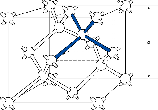
This periodic arrangement of atoms is called crystal structure. For an introduction to crystals, interested readers can refer to the previous chapters.
5. Key Points Related to Semiconductors
(1) Energy Levels and Energy Bands
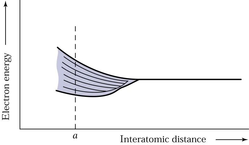
We can imagine atoms as planets, and the electrons surrounding the atoms as satellites orbiting around the planets.
In the galaxy, when two planets are far enough apart, they can be considered to have the same energy. As two planets gradually approach each other, the interaction between them, including the attractive and repulsive forces between any two planets, will cause the energy levels to shift.
Unlike when only two planets are involved, where the energy levels simply divide into two, when many planets in the galaxy come close, the energy levels will split into N separate but close levels. When N is large, a continuous energy band is formed, and these N energy levels can extend over several electron volts, depending on the distance between the planets.
The diagram below describes the relationship between the distance of planets (atoms) and energy levels:
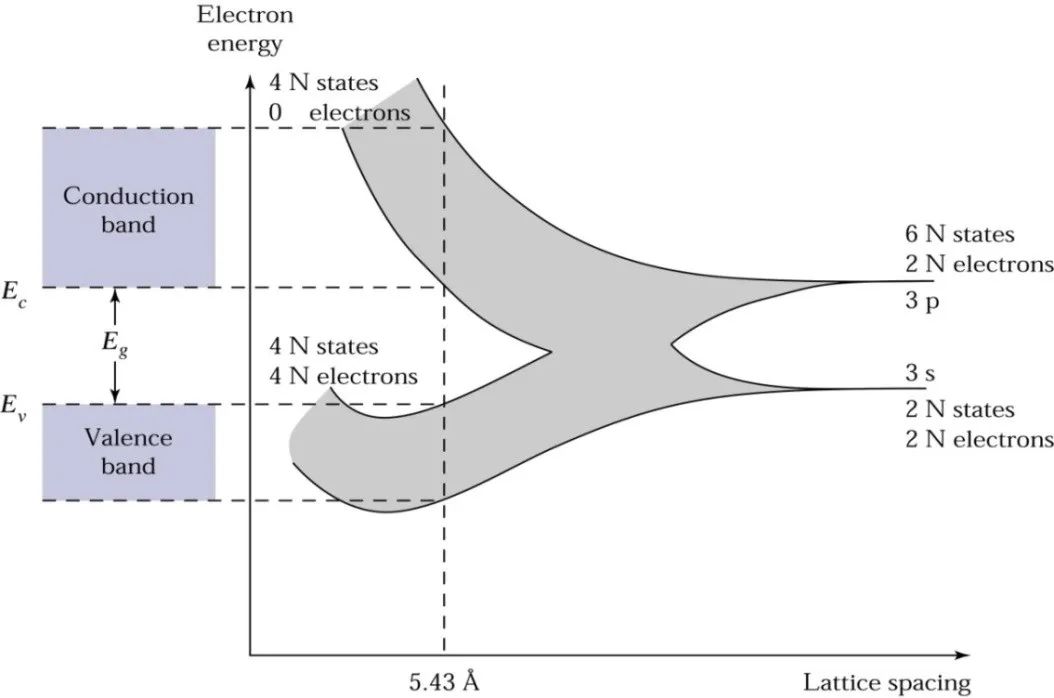
Now returning to the atomic arrangement of silicon wafer, under equilibrium conditions, the atomic distances will cause the energy bands to split again, resulting in each atom having four quantum states in the lower energy band and four quantum states in the higher energy band.
At absolute zero, electrons occupy the lowest energy states, so all energy states in the lower energy band (the valence band) will be filled with electrons, while in the higher energy band (the conduction band), there will be no electrons. The bottom of the conduction band is called Ec, and the top of the valence band is called Ev.
The energy gap between the bottom of the conduction band and the top of the valence band (Ec – Ev) is called the bandgap width Eg.
As shown in the diagram below, in physical terms, Eg represents the energy required to break an electron in the semiconductor valence band, turning it into a free electron and moving it to the conduction band, leaving a hole in the valence band.
The kinetic energy of a free electron can be expressed as:
E=P2/2M
Where p is the momentum and m is the mass of the free electron.
Plotting E against p will yield a parabolic graph as shown below.
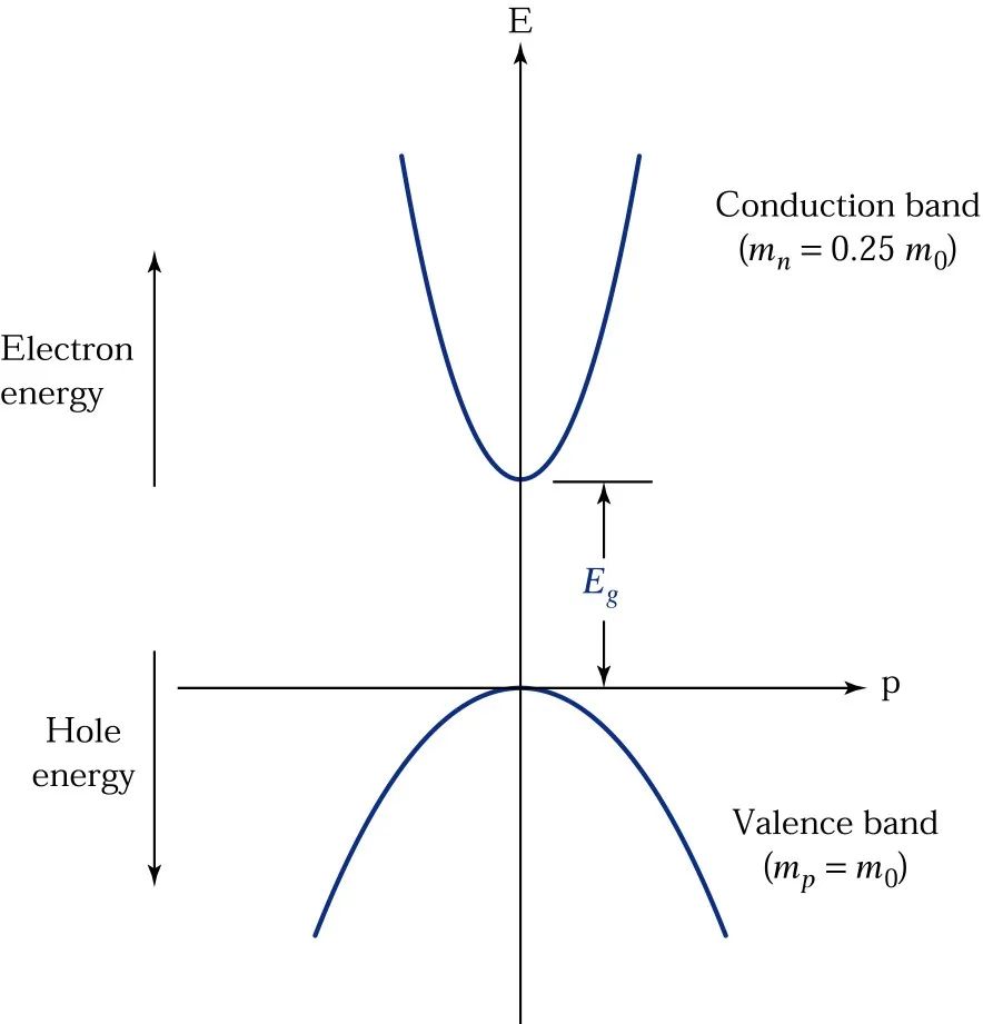
For silicon, its momentum and energy curve peaks at p=0 for the top of the valence band, while the lowest point of the conduction band occurs at p=pC along the [100] direction. Therefore, when an electron transitions from the top of the valence band to the lowest point of the conduction band, not only energy conversion (≥Eg) is required, but also momentum conversion (≥pC) is needed, as shown in the diagram (a).
This type of semiconductor is called an indirect bandgap semiconductor.
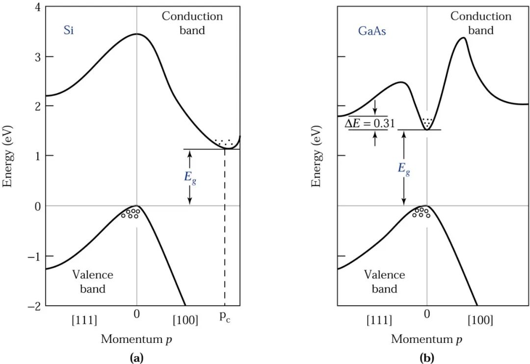
The diagram (b) shows the momentum-energy relationship curve for Gallium Arsenide, where the top of the valence band and the lowest point of the conduction band occur at the same momentum (p=0). Therefore, when an electron transitions from the valence band to the conduction band, no momentum conversion is necessary.
This type of semiconductor is called a direct bandgap semiconductor.
(2) Conductors, Semiconductors, Insulators
There are significant differences in electrical conductivity among metals, semiconductors, and insulators, which can be qualitatively explained using their energy bands. It has been found that the occupancy of electrons in the highest energy band or the highest two energy bands determines the conductivity of the solid.
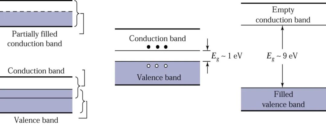
Conductors (metals): Metal conductors have very low resistance, and their conduction band is either partially filled [like copper (Cu)] or overlaps with the valence band [like zinc (Zn) or lead (Pb)], so there is essentially no bandgap present, as shown in the diagram.
Thus, electrons in the highest occupied states of the partially filled conduction band or the top of the valence band can move to the next higher energy state when they gain kinetic energy (for example, from an external electric field). For metals, since there are many unoccupied energy states near the states close to full occupancy, even a small external electric field allows electrons to move freely, which is why metal conductors can easily conduct electricity.
Insulators: Insulators like silicon dioxide (SiO2) have very strong covalent bonds formed between the valence band electrons and neighboring atoms. These bonds are difficult to break, so at room temperature or near room temperature, there are no free electrons participating in conduction, as shown in the diagram.
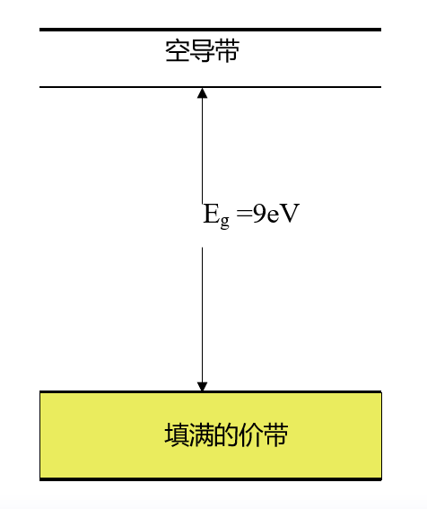
The characteristic of insulators is a large bandgap width, as seen in the diagram where the energy levels in the valence band are fully occupied, while the energy levels in the conduction band are empty. Thermal energy or energy from an external electric field is insufficient to excite the electrons at the top of the valence band to the conduction band. Therefore, although there are many empty energy states in the conduction band that could accept electrons, in reality, very few electrons can occupy the energy states in the conduction band, contributing very little to conductivity, resulting in high resistance and inability to conduct electricity.
Semiconductors: Semiconductor materials have conductivity between that of conductors and insulators, and they are easily affected by temperature, light, magnetic fields, and minute impurities, with a smaller bandgap width (approximately 1 eV), as shown in the diagram.
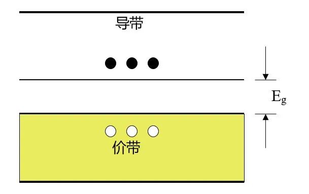
At T=0K, all electrons are located in the valence band, and there are no electrons in the conduction band, thus semiconductors are poor conductors at low temperatures. At room temperature and normal atmospheric pressure, the Eg value of silicon is 1.12eV, while that of Gallium Arsenide is 1.42eV. Therefore, at room temperature, thermal energy kT occupies a certain proportion of Eg, allowing some electrons to be excited from the valence band to the conduction band. Because there are many unoccupied energy states in the conduction band, only a small amount of external energy is needed to easily move these electrons, generating a considerable electric current.
(3) Intrinsic Semiconductors:
When the concentration of impurities in a semiconductor is much smaller than the electrons and holes generated by heat, this type of semiconductor is called an intrinsic semiconductor.
(4) Extrinsic Semiconductors:
When a semiconductor is doped with impurities, it becomes extrinsic, introducing impurity energy levels.
Intrinsic semiconductors can be understood as a dish of stir-fried cabbage without adding any seasonings, where the flavor of the cabbage itself remains unchanged, referred to as intrinsic.
Extrinsic semiconductors can be understood as the same stir-fried cabbage, but with different seasonings added, resulting in a dish with different flavors.
It is precisely because different seasonings yield different flavors that the application of doping in semiconductors has become more widespread.
(5) Donors:
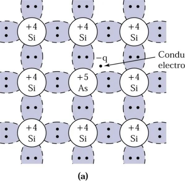
We know that wafers are composed of silicon atoms, and silicon has four electrons in its outer shell. Someone thought of an idea: if arsenic, which has five valence electrons, is added to the wafer, a silicon atom can be replaced (or substituted) by an arsenic atom with five valence electrons. This arsenic atom forms covalent bonds with four neighboring silicon atoms, and its fifth electron has a relatively small binding energy, allowing it to be ionized into a conduction electron at an appropriate temperature.
Typically, we say this electron is donated to the conduction band, and the arsenic atom is referred to as a donor. Due to the increase in negatively charged carriers, silicon becomes an n-type semiconductor (the first letter of the English word Negative), as illustrated in the diagram:
(6) Acceptors:
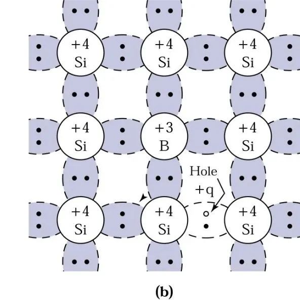
Similarly, in a wafer composed of silicon atoms, when a boron atom with three valence electrons replaces a silicon atom, it needs to accept an additional electron to form four covalent bonds around the boron atom, resulting in a positively charged hole in the valence band.
This is referred to as a p-type (Positive) semiconductor, and the boron atom is called an acceptor.
6. Motion of Electrons in Semiconductors
The conduction electrons in the conduction band of semiconductors are not bound to any specific lattice or donor positions, so they are essentially free particles. Under thermal equilibrium, a conduction electron exhibits thermal motion (velocity vth). At room temperature, the thermal motion velocity of electrons in silicon and gallium arsenide is approximately 10E7 cm/s.
Electrons in semiconductors move rapidly in all directions, as shown in the diagram below.
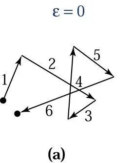
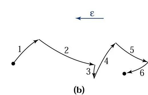
When a small electric field E is applied to the semiconductor sample, each electron will experience a force of qE from the electric field, accelerating in the opposite direction during collisions. Therefore, an additional velocity component will be added to the thermally moving electrons, and this additional velocity component is called drift velocity.
The displacement of an electron caused by both random thermal motion and drift components is illustrated in the diagram below.
It is important to note that the net displacement of electrons is in the opposite direction of the applied electric field (because electrons are negatively charged).
This directional movement of carriers under the influence of an external electric field is referred to as drift motion.
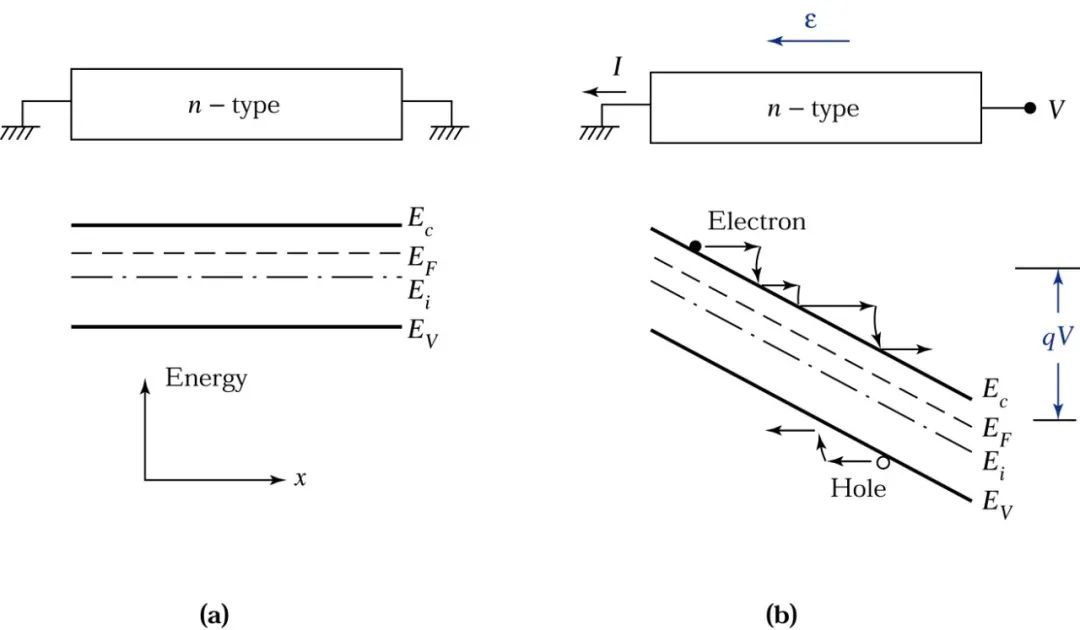
The diagram (a) shows an n-type semiconductor and its energy band diagram under thermal equilibrium. Diagram (b) shows the corresponding energy band diagram when a voltage is applied to the right end.
Assuming that both the left and right contact surfaces are ohmic contacts, the transport of carriers under the influence of an external electric field generates a current, known as drift current.
(7) Hall Effect
In a semiconductor, the concentration of carriers may differ from the concentration of impurities because the ionized impurity concentration depends on temperature and impurity energy levels. The most common method to directly measure carrier concentration is the Hall effect. Hall measurement is also one of the most convincing methods to demonstrate the existence of holes as charged carriers since the measurement itself can directly determine the type of carriers.
Measurement Method: Consider applying an electric field along the x-axis and a magnetic field along the z-axis to a p-type semiconductor sample, as shown in the diagram.
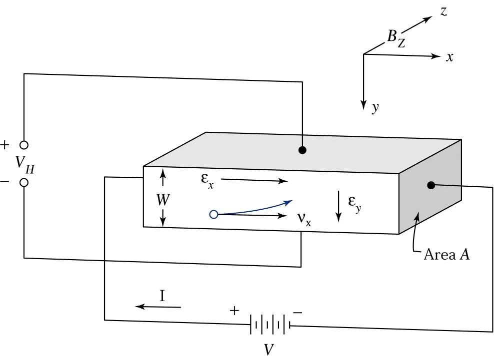
The Lorentz force qv×B (=qvxBz) generated by the magnetic field will exert an upward force on the holes flowing in the x-axis direction, causing the holes to accumulate above the sample, thus generating a downward electric field Ey.
Once the electric field Ey becomes equal to vxBz, the holes will not experience a net force in the y-axis direction while drifting along the x-axis. The establishment of this electric field is known as the Hall Effect. The electric field in the above equation is referred to as the Hall Electric Field, and the voltage across the two ends VH=EyW is referred to as the Hall Voltage.
(8) Avalanche Process:
When the electric field in the semiconductor exceeds a certain value, carriers gain sufficient kinetic energy to generate electron-hole pairs through the avalanche process, as illustrated in the diagram below.
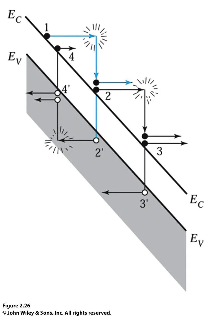
Consider an electron in the conduction band, assuming the electric field is sufficiently high, this electron can gain kinetic energy before colliding with the lattice. When it collides with the lattice, the electron loses most of its kinetic energy to break chemical bonds, thereby ionizing a valence electron from the valence band to the conduction band, generating an electron-hole pair 2 and 2′. The generated electron-hole pairs begin to accelerate in the electric field and collide with the lattice, producing additional electron-hole pairs 3 and 3′ and 4 and 4′, and so on. This process is called the avalanche process, also known as the impact ionization process, which leads to the breakdown of the p-n junction.
After breakdown, the conductivity of the semiconductor changes, losing its semiconductor characteristics, resulting in device failure.
END
The reproduced content represents the author’s viewpoint only.
It does not represent the position of the Semiconductor Institute of the Chinese Academy of Sciences.
Editor: Xiaoshuai
Responsible Editor: Liu Kuai Qian’s Fish
Submission Email: [email protected]
1. Progress in Research on Biomimetic Covering Neuron Models and Learning Methods in Semiconductors
2. Significant Progress in Inverted Structure Perovskite Solar Cells in Semiconductors
3. Why is Copper Used as Interconnect Metal in Chips?
4. What is the 7nm in Chips?
5. Silicon-based Integrated Optical Quantum Chip Technology
6. How Abnormal is the Quantum Anomalous Hall Effect? It Might Bring the Next Revolution in Information Technology!