Infrared (IR) sensors are widely used in various scenarios due to their ability to detect infrared radiation. Currently, infrared detector technology has entered its third generation and is facing significant challenges. The propagation of infrared radiation can be divided into different optical windows, with the mid-wave infrared (MWIR) and long-wave infrared (LWIR) bands being the most valuable for research in the field of infrared thermal imaging. Infrared thermal imaging detectors are extensively applied in consumer, industrial, security, search and rescue, monitoring, and medical fields. Currently, high-performance infrared imaging technology mainly relies on the epitaxial growth structures of narrow bandgap semiconductor alloys such as mercury cadmium telluride (MCT), indium antimonide (InSb), and gallium arsenide (GaAs) based quantum well infrared photodetectors (QWIP), with specific choices depending on the application scenario and wavelength range. Nanostructures and nanomaterials with suitable electrical and mechanical properties, including two-dimensional materials, graphene, quantum dots (QD), dot-in-well (DWELL), and colloidal quantum dots (CQD), will significantly enhance the electronic characteristics of infrared photodetectors, transition metal dichalcogenides, and metal oxides, which are attracting significant attention from researchers.
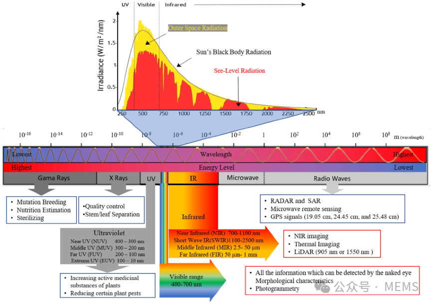
Figure 1 Electromagnetic spectrum and its representative regions, energy levels, and application examples
According to a report by MEMS Consulting, a team of researchers from institutions such as MAT4NRG GmbH in Germany, KU Leuven in Belgium, and the National Technical University of Athens (NTUA) in Greece published a review paper titled “IR Sensors, Related Materials, and Applications” in the journal Sensors, detailing the research progress in infrared sensors. This paper comprehensively introduces the types of infrared sensors, commonly used materials, and related application examples.
Types of Infrared Sensors
Devices that detect infrared radiation can be divided into three categories: photon detectors, thermal detectors, and radiation field detectors. Based on their working principles, infrared sensors can mainly be classified into thermal and quantum types. Thermal sensors convert infrared light into thermal energy, which is then output as a signal through changes in resistance and thermoelectric potential. Quantum sensors primarily utilize the photoconductive effect of semiconductor transition energy and the photovoltaic effect of PN junctions. Pyroelectric infrared sensors belong to thermal sensors.
Infrared sensors can be classified into active and passive types based on the presence of a light source. Active infrared sensors (AIR) emit and receive in the infrared band (as shown in Figure 2), consisting of a light source and a detector; when an object approaches the active sensor, the infrared light emitted by the light source is reflected by the object and captured by the detector. Active infrared sensors are commonly used as proximity sensors in obstacle detection systems for robots. Passive infrared sensors are specifically designed for detecting infrared radiation without a light source; passive infrared sensors (PIR) consist of two layers of pyroelectric materials (pyroelectric sensors), infrared filters (to filter out other wavelengths), Fresnel lenses (to focus multi-angle light onto a single point), and housing units (to protect the sensor from environmental variables such as temperature and humidity). Passive infrared sensors are mainly applied in motion detection systems based on passive infrared technology.
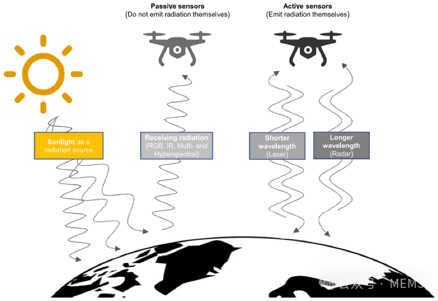
Figure 2 Schematic diagram of a drone equipped with active and passive infrared sensors
The performance of photoconductive detectors, photovoltaic detectors, and photoelectromagnetic detectors essentially depends on the lifetime of the photo-excited carriers. In photon detectors, incident photons are absorbed through interaction with electrons, which may be related to lattice atoms, impurity atoms, or even free electrons. The measured signal comes from changes in the electronic energy level distribution. Figure 3 illustrates the basic photo-excitation mechanisms in semiconductors.
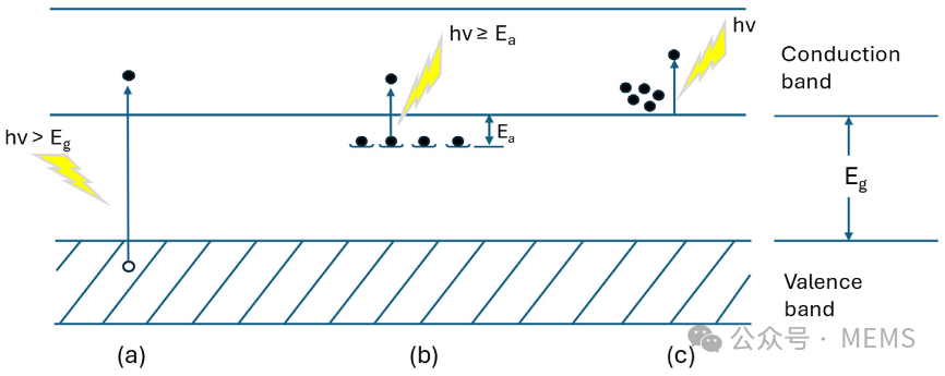
Figure 3 Basic photo-excitation processes in semiconductors: (a) intrinsic absorption; (b) extrinsic absorption; (c) free carrier absorption.
Materials for Infrared Sensors
Organic materials have become an important research topic for sensitive materials in pyroelectric infrared sensors. With the development of polymer-based materials, many functional polymer materials have also exhibited ferroelectric, piezoelectric, and pyroelectric properties. Polyvinylidene fluoride (PVDF) is one of the most studied pyroelectric materials. Several studies have used PVDF and P(VDF)-TrFE and other organic-inorganic composite materials as matrices, combined with insulating lead zirconate titanate (PZT), for use in piezoelectric and pyroelectric sensors. Research on infrared sensors using organic and carbon-based materials is shown in Figures 4 and 5.
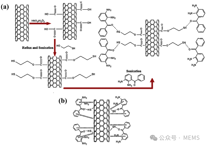
Figure 4 (a) Functionalization and crosslinking reaction scheme of multi-walled carbon nanotubes (MWCNT); (b) π-π stacking scheme.
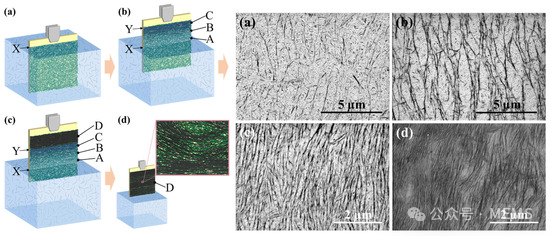
Figure 5 Scanning electron microscope (SEM) images of the preparation process of bilayer films and the attachment process of single-walled carbon nanotubes (SWCNT) on wet (left) and dry (right) surfaces
In recent years, pyroelectric infrared sensors using PZT films have gained significant attention in military, homeland security, and civilian fields due to their cost-effectiveness, compact structure, wide spectral response, and reliability superior to traditional photon infrared detectors. Research on infrared sensors based on PZT films mainly involves night vision imaging, gas monitoring, and motion sensing.
Uncooled Schottky phototuned barrier detectors (SPBD) can break through the internal light emission limit to achieve ultra-sensitive broadband light detection capabilities. The SPBD structure includes a graphene-silicon Schottky junction for carrier suppression and narrow bandgap lead telluride (PbTe) for infrared light absorption. The optical response principle of SPBD fundamentally differs from that of traditional Schottky infrared detectors (as shown in Figure 6), which is due to the dynamic changes of the Schottky barrier under infrared light illumination. Figures 6A and 6B compare the working mechanism differences between SPBD and traditional light-emitting detectors.
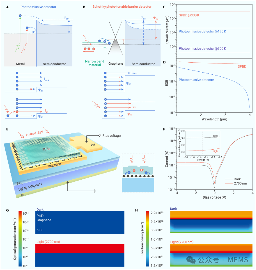
Figure 6 Comparison of SPBD and traditional Schottky infrared detectors
The quantum dot system exhibits zero-dimensional quantum confinement effects. In the absence of external influences, carriers will be confined within the three-dimensional space of the quantum dots. Carriers will be restricted to designated areas within the semiconductor device. Additionally, by adjusting external variables such as electric fields and device temperatures, carriers can be selectively captured or released. Quantum dot infrared photodetectors (QDIP) operate on principles similar to QWIP but can address related issues through zero-dimensional quantum confinement mechanisms. Multi-quantum dot material systems exhibit type-II band alignment, such as GaAs quantum dots deposited on indium arsenide (InAs) substrates or InSb quantum dots deposited on InAs substrates.
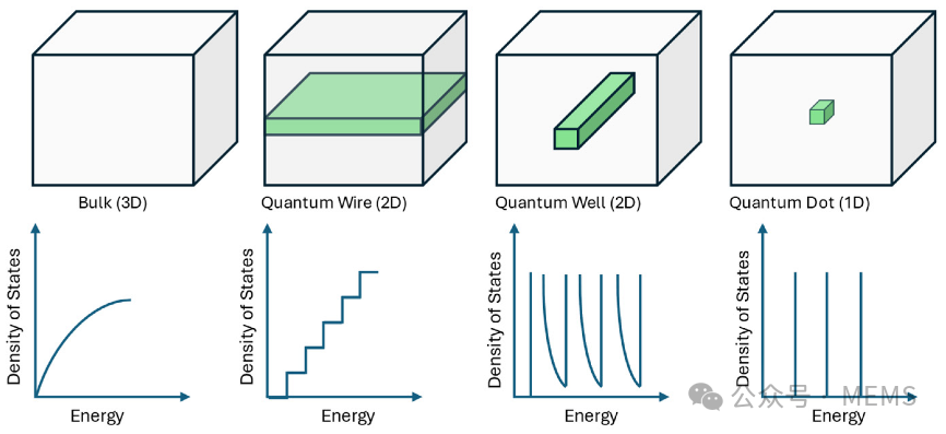
Figure 7 Schematic diagram of the spatial distribution and density of states of bulk materials, quantum wells, quantum wires, and quantum dots
A quantum well is an ultra-thin layer of semiconductor material “sandwiched” between two layers (or two three-dimensional bulk materials) of another material. Carriers are confined within this plane but can move within it. The QWIP technology based on subband transitions has attracted significant attention in thermal imaging applications in the mid-wave infrared and long-wave infrared spectral ranges over the years, utilizing III-V heterostructures. QWIP is crucial for long-wave infrared photon-dense systems, covering fields such as medical imaging, gas detection, and monitoring applications. However, it faces issues such as low quantum efficiency, high dark current, lack of typical incident absorption, and the need for low operating temperatures.
A hybrid structure combining the characteristics of QWIP and QDIP, proposed several years ago, is known as dot-in-well (DWELL). This structure exhibits multiple advantages, including voltage-dependent multispectral response characteristics. The active part of DWELL consists of InAs quantum dots embedded within InGaAs quantum wells, achieving a fusion of traditional QWIP and QDIP. The DWELL structure possesses multiple advantages, with multispectral response characteristics similar to QWIP, voltage-dependent spectral tunability, and repeatable wavelength control capabilities. Additionally, DWELL combines low dark current with the vertical incident working mode of QDIP. The multispectral response arises from various transition energy levels, including transitions between quantum dots, transitions from quantum dots to quantum wells, and transitions from quantum dots to continuous energy bands. Its spectral tunability is achieved through band bending, which is influenced by the bias voltage that alters the transition energy.
Type-II InAs/GaInSb superlattice structures (T2SL) are a new alternative infrared material system that shows great potential in the long-wave infrared/very long-wave infrared (VLWIR) spectral range, with performance comparable to HgCdTe materials at equivalent cutoff wavelengths. The type-II InAs/GaSb superlattice structures fabricated on GaSb substrates, with their superior spatial uniformity and precise cutoff wavelength tuning capabilities, have become strong alternatives to mainstream MCT photodiodes and quantum well infrared photoconductors. T2SL photodiodes typically adopt a P-i-N structure, characterized by an intrinsic region (ν or π region) with incidental doping between heavily doped p-type and n-type materials with a larger bandgap and lattice matching. The reduction of minority carrier concentration in the high bandgap layer can decrease diffusion current, improve RoA values, and enhance detection sensitivity.
Sub-monolayer quantum dots (SML QD) have gained attention as an alternative for quantum dot fabrication due to their ability to generate high-density uniform quantum dots. Compared to traditional S-K QDIP, infrared photodetectors using multilayer stacked SML quantum dots exhibit enhanced device performance: reduced dark current density, improved responsivity, and increased detectivity. Furthermore, by constructing suitable AlGaAs barriers, the performance of SML QDIP can be significantly improved, facilitating the realization of excellent quantum confinement effects for carriers.
Applications of Infrared Sensors
Infrared sensors are widely used in consumer, industrial, security, search and rescue, monitoring, medical, research, meteorology, climatology, and astronomy fields.
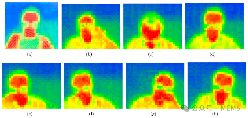
Figure 8 Output images of various sitting posture detections
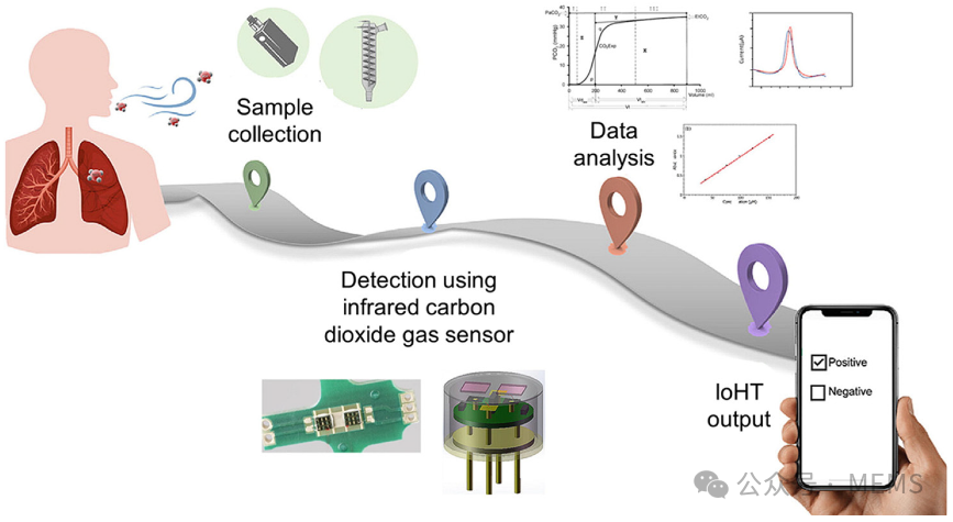
Figure 9 Architecture for monitoring respiratory diseases using easily accessible human exhaled gases combined with infrared CO₂ gas sensors
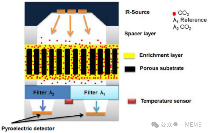
Figure 10 Schematic diagram of a micro infrared CO₂ sensor with an enrichment layer
In summary, the application prospects of infrared detection systems must meet the following requirements: enhance pixel sensitivity, increase pixel density; significantly reduce the cost of infrared imaging array systems through more efficient or uncooled detector technologies, as well as integrating detectors with signal processing functions (significantly enhancing on-chip signal processing); and improve the functionality of infrared imaging arrays by developing multispectral sensors. The future vision for the development of infrared detector technology includes combining photodetectors with advanced electronic devices that execute complex algorithms, where artificial intelligence (AI) may become an important tool for adaptive systems.
Paper link:
https://doi.org/10.3390/s25030673