Infrared optoelectronic sensors have attracted significant research attention over the past few decades due to their wide applications in military defense, biomedical, environmental monitoring, industrial inspection, and human-computer interaction systems. A comprehensive understanding of infrared optoelectronic sensors is crucial for achieving their future optimization.
According to a report by MEMS Consulting, researchers from Beihang University and the National University of Singapore jointly published a review article titled “Progress in Advanced Infrared Optoelectronic Sensors” in the journal Nanomaterials. The article provides a comprehensive overview of the latest advancements in infrared optoelectronic sensors. It first clarifies their working mechanisms, then introduces the key performance indicators for evaluating infrared optoelectronic sensors, followed by an overview of promising materials and nanostructures for high-performance infrared optoelectronic sensors, and the performance of state-of-the-art sensors. Finally, it points out the challenges faced by infrared optoelectronic sensors and discusses optimization directions, paving the way for the future development of infrared optoelectronic sensors.
I Working Mechanisms
The photovoltaic effect refers to the phenomenon where electron-hole pairs generated by light excitation are driven, separated, and transported under an internal electric field, resulting in an electrical signal. Based on the photovoltaic effect, infrared optoelectronic sensors absorb photons to generate electron-hole pairs, which are then extracted and accelerated by the internal electric field, producing a significant photocurrent/photovoltaic signal. Their internal electric field mainly arises from the formation of depletion regions at the Schottky junction, semiconductor homojunctions/heterojunctions, and semiconductor/electrolyte junction interfaces.
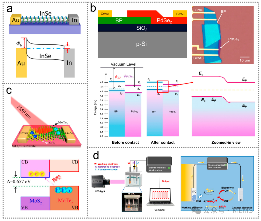
Working mechanism of photon-type infrared optoelectronic sensors
The photoconductive effect refers to a phenomenon where the conductivity of a semiconductor changes with the intensity of incident light. In infrared optoelectronic sensors based on the photoconductive effect, the generation of electrical signals is very similar to that based on the photovoltaic effect, where photogenerated electron-hole pairs are produced by photon absorption. However, in photoconductive sensors, the separation and transport of photogenerated electron-hole pairs require an external electric field as the driving force.
The pyroelectric effect refers to the phenomenon of charge generation in response to changes in spontaneous polarization caused by temperature variations, which typically occurs in certain polar materials. Pyroelectric infrared optoelectronic sensors have several advantages over other types of sensors, such as room temperature operation, wide wavelength response, and low cost, making them suitable for various consumer applications.
The photothermal effect utilizes the coupling of photothermal and thermoelectric effects in semiconductors to generate electric potential. The figure below shows a typical photothermal infrared optoelectronic sensor, which has a planar device configuration with electrodes located at both ends of the semiconductor. In addition to n-type or p-type semiconductors, photothermal infrared optoelectronic sensors can also be constructed by utilizing p-n junctions in certain materials.
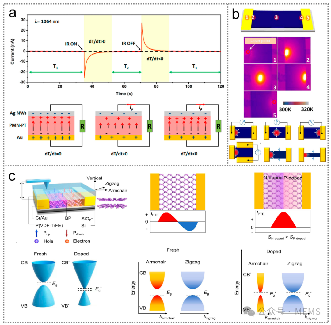
Working mechanism of photothermal infrared optoelectronic sensors
By leveraging the advantages of the photovoltaic effect and the photothermal effect, infrared optoelectronic sensors can be constructed based on the pyroelectric-photovoltaic effect, which is the coupling of pyroelectric polarization, semiconductor/ferroelectric characteristics, and the light excitation process. Since the light-induced photovoltaic signal and thermoelectric signal have the same polarity, the electrical signal of pyroelectric-photovoltaic infrared optoelectronic sensors can achieve enhanced infrared response compared to infrared optoelectronic sensors based solely on the pyroelectric effect or photovoltaic effect. The pyroelectric-photothermal effect is another important mechanism for constructing infrared optoelectronic sensors, as it maximizes the utilization of light-induced heat to generate electrical signals.
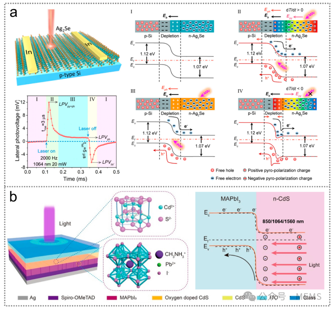
Working mechanism of infrared optoelectronic sensors based on coupling effects
II Key Performance Indicators
The key parameters for evaluating the performance of infrared optoelectronic sensors include their spectral response range, responsivity (R), response speed, gain (G), noise equivalent power (NEP), specific detectivity (D*), on/off ratio (Rratio), linear dynamic range (LER), and external quantum efficiency (EQE).
III Materials and Their Performance
Two-dimensional materials have great potential for constructing highly integrated and efficient infrared optoelectronic sensors due to their tunable bandgap, high carrier mobility, and strong light absorption characteristics. Since the photon energy corresponding to the infrared band is relatively low (about 1.55 eV), the two-dimensional materials used in infrared optoelectronic sensors are mostly semimetals and narrow bandgap semiconductors. Semimetals represented by graphene, TaAs, PdTe₂, WTe₂, and TaIrTe have a gapless linear cone-shaped electronic band structure, enabling broadband infrared sensing extending into the far-infrared spectrum. The photogenerated carriers in semimetals can significantly shorten their lifetime through rapid electron-electron scattering, thus achieving fast response. However, due to the gapless characteristics, infrared optoelectronic sensors based on semimetals typically suffer from high dark current issues. Narrow bandgap two-dimensional semiconductors such as black phosphorus (BP), black arsenic phosphorus (B-AsP), bismuth selenide (Bi₂Se₃), tellurene, metal chalcogenides, and transition metal dichalcogenides have tunable bandgaps that help reduce dark current. Among these two-dimensional materials, graphene, black phosphorus (BP), and metal chalcogenides are the most commonly used materials for fabricating infrared optoelectronic sensors.
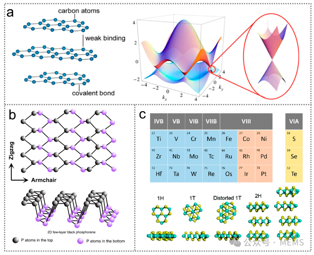
Two-dimensional materials for infrared optoelectronic sensors
Narrow bandgap III-V semiconductors are widely used for constructing infrared optoelectronic sensors due to their high carrier mobility, excellent stability, low dielectric constant, and high absorption coefficient. To date, III-V semiconductor quantum dots, thin films, and single-crystal nanowires have been developed to achieve high-performance infrared sensing. Compared to infrared sensors based on single-crystal nanowires, those based on III-V semiconductor quantum dots and thin films typically exhibit relatively poorer performance due to the numerous bulk and surface defects generated during the fabrication process. Single-crystal nanowires can transport charge carriers along their axial direction, reducing carrier scattering and trapping, thereby improving device performance.
Ferroelectric materials have become key materials for manufacturing infrared optoelectronic sensors due to their significant pyroelectric effect and anomalous photovoltaic effect. Compared to other types of thermoelectric materials, ferroelectric materials have unique advantages, such as high thermoelectric coefficients, excellent chemical and mechanical stability, and low manufacturing costs. Additionally, some ferroelectric materials have narrow bandgaps, making them suitable for simultaneously utilizing both thermoelectric and photovoltaic effects to detect infrared light. A class of ferroelectric materials that has emerged for infrared sensing applications is molecular perovskite materials, which exhibit strong structural flexibility, such as metal halide perovskites, metal formates, and non-metal molecular perovskites.
Organic semiconductor materials are attractive candidates for constructing infrared optoelectronic sensors due to their inherent flexibility, lightweight, low cost, scalability, and ease of fabrication. Furthermore, organic semiconductor materials can enable uncooled infrared sensing, thus holding great potential for future wearable devices. Significant efforts have been made to explore organic semiconductor materials suitable for high-performance infrared optoelectronic sensors. Currently, research on organic semiconductor materials for infrared optoelectronic sensors mainly focuses on developing narrow bandgap organic polymers and small molecules.
In addition to the advanced materials mentioned above that have been widely studied, other materials have also been used to construct high-performance infrared optoelectronic sensors, such as mercury chalcogenides and organic-inorganic hybrid perovskite semiconductors. Mercury chalcogenides exhibit unique ultra-broad and tunable optical responses in the near-infrared and mid-infrared regions, demonstrating photodetection performance comparable to commercial devices, particularly advantageous at high temperatures. Organic-inorganic hybrid perovskite semiconductors are considered one of the most promising materials for infrared sensing applications due to their long exciton diffusion lengths, high carrier mobility, direct bandgap, and high absorption coefficients.
III Applications
Infrared optoelectronic sensors have deeply integrated into modern technology and human society, with applications spanning image sensing, optical neuromorphic computing, logic operations, and health monitoring.
Imaging is one of the most widespread applications of infrared optoelectronic sensors, with numerous imaging devices developed based on different materials. Infrared polarization imaging sensors can extend the detection range of photonic signals from the wavelength and intensity of light to the polarization vector of light, showing great potential in remote sensing imaging, medical diagnostics, and environmental monitoring. In addition to the aforementioned planar imaging sensors, infrared optoelectronic sensors can also be designed as hemispherical devices for wide-angle imaging applications.
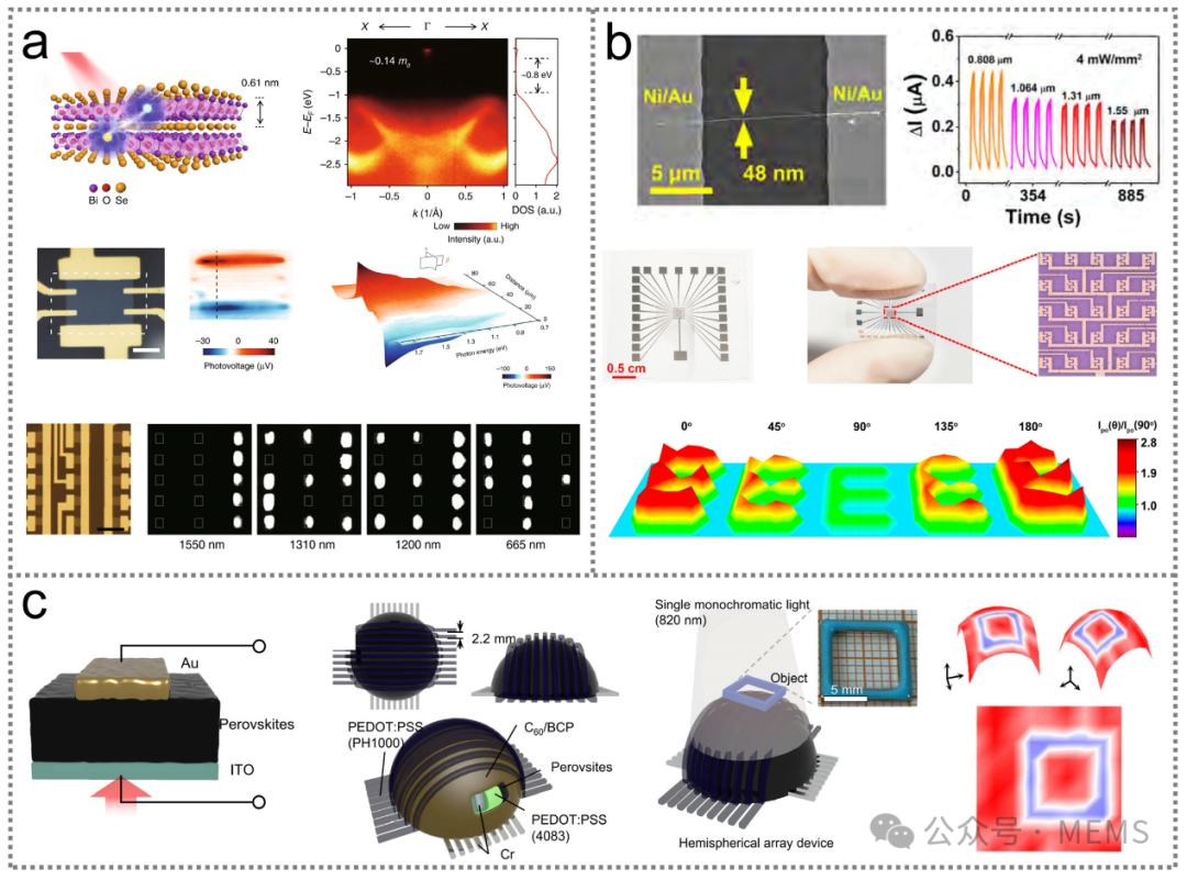
Infrared optoelectronic sensors for imaging
Neuromorphic optoelectronic sensors utilize artificial light-sensitive synapses, capable of simulating biological neural systems, with memory perception and computational capabilities. Based on a planar heterostructure composed of perylene and graphene oxide, the optoelectronic sensor exhibits a broadband light sensing range from 0.365 μm to 1.55 μm and an ultra-high specific detectivity of 3.1 × 10¹³ Jones. Furthermore, infrared optoelectronic sensors can also be used for edge computing (computation within the sensor), significantly reducing communication latency and energy consumption in distributed systems and robotic devices.
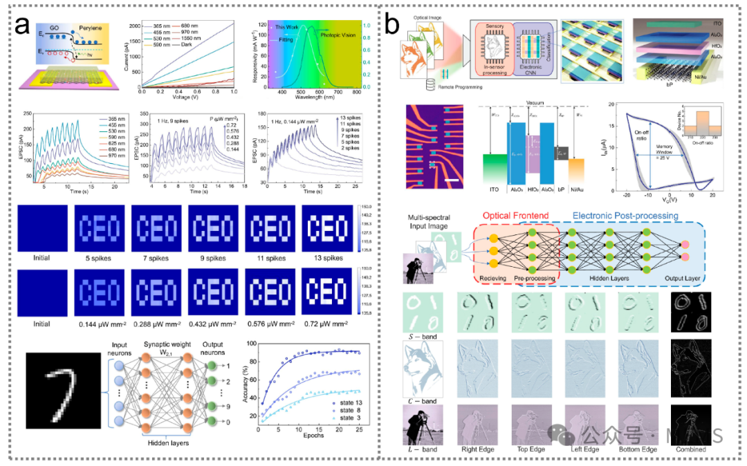
Infrared optoelectronic sensors for neuromorphic computing
The growing demand for extensive data processing has driven interest in optoelectronic logic gate platforms due to their wide bandwidth and fast data transmission. Optoelectronic sensors based on back-to-back p+-i-n-p-p+ diode structures exhibit bipolar spectral optical responses to visible and infrared light. When illuminated by visible and infrared light, the sensor generates positive and negative currents, respectively, paving the way for optical logic gate operations.
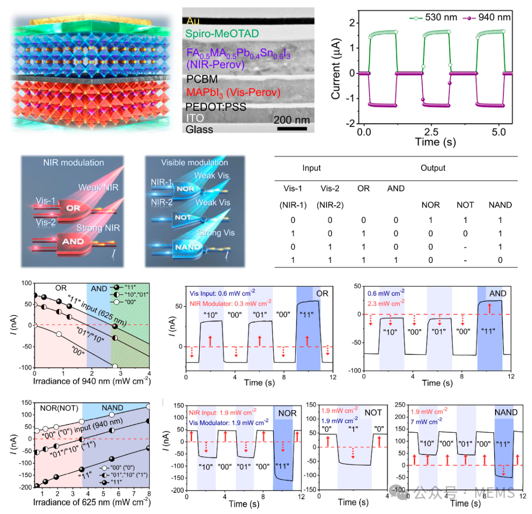
Device design and output characteristics of perovskite infrared optoelectronic sensors for logic operations
Infrared optoelectronic sensors provide an effective means for health monitoring, particularly for pulse frequency and blood oxygen saturation (SpO₂). The figure below shows a flexible optoelectronic sensor based on metal halide perovskite, which can be used for pulse signal detection based on photoplethysmography.
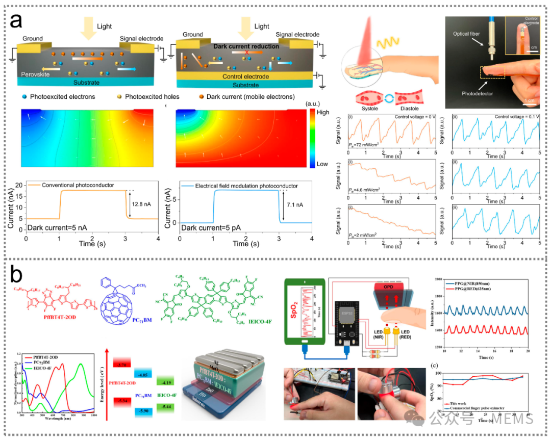
Infrared optoelectronic sensors for health monitoring
In addition to the aforementioned applications, infrared optoelectronic sensors also demonstrate potential applications in optical communication and gas sensing.
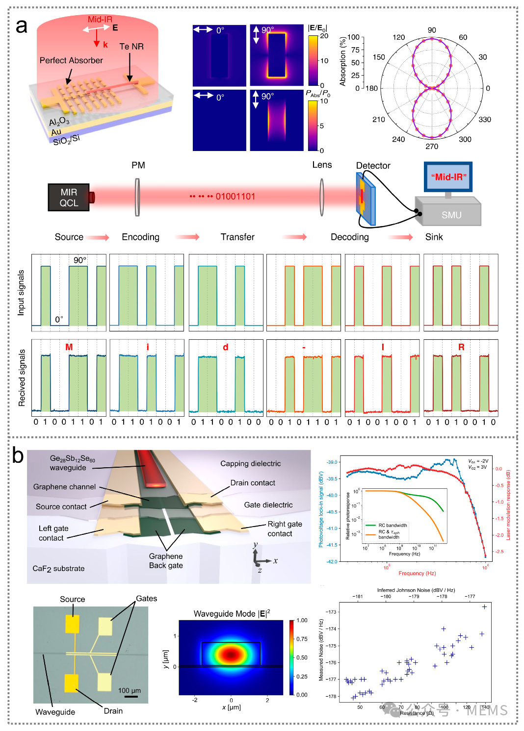
Infrared optoelectronic sensors for optical communication and gas sensing
In summary, this article reviews the research progress of infrared optoelectronic sensors. Based on their working mechanisms, these sensors can be roughly divided into three categories: photon-type sensors, photothermal-type sensors, and hybrid-type sensors. Two-dimensional semimetals and semiconductors, III-V semiconductors, ferroelectric materials, and organic semiconductors exhibit unique advantages in infrared optoelectronic sensing. For example, two-dimensional semimetals and semiconductors are suitable for high-speed photodetection due to their high carrier mobility, while ferroelectric materials have the potential to enhance light response by simultaneously utilizing both pyroelectric and photovoltaic effects. Infrared optoelectronic sensors are deeply integrated into modern technology and human society, with broad application prospects in imaging, neuromorphic computing, logic operations, optical communication, health monitoring, and gas sensing.
Despite the significant progress made in the research of infrared optoelectronic sensors, several challenges remain in the field. (1) The response speed of most existing infrared optoelectronic sensors is in the microsecond range, which is insufficient to capture rapidly changing light. (2) Comprehensive characterization of infrared optoelectronic sensors is needed to further optimize devices, including their response range, responsivity, specific detectivity, response time, NEP, LDR, and EQE. (3) Although some infrared optoelectronic sensors have been used for health monitoring applications, there is a lack of research on their biocompatibility.
Considering the growing demand for high-performance infrared optoelectronic sensors, various research directions can be pursued in the near future to advance the development of infrared optoelectronic sensors. (1) Most two-dimensional materials used for infrared optoelectronic sensors are manufactured based on small-sized mechanically exfoliated flakes, so developing scalable production techniques is crucial. The most promising methods for achieving large-scale two-dimensional materials may be CVD and molecular beam epitaxy. (2) Infrared optoelectronic sensors based on narrow bandgap semiconductors often exhibit unstable performance due to variations in environmental temperature, so developing temperature-insensitive devices is of great significance. Miniature temperature control systems integrated into infrared optoelectronic sensors can help address this issue. (3) The development of optical logic operations and optical communication poses new challenges for high-frequency devices, thus ultra-fast infrared optoelectronic sensors are ideal. To achieve this goal, materials with ultra-high carrier mobility and homojunction/heterojunction structures with strong built-in electric fields are needed. (4) Research on biocompatible infrared optoelectronic sensors has broad application prospects in future healthcare, which can be achieved by using non-toxic organic semiconductors. (5) In optical neuromorphic computing applications, developing light synapses for weight storage with long memory characteristics is crucial. Utilizing device interfaces or ferroelectric polarization to achieve carrier trapping is expected to achieve this goal. Overall, the development of infrared optoelectronic sensors will drive advancements in daily life, industry, and healthcare, and further efforts are needed to enhance their performance.
Paper link:
https://www.mdpi.com/2079-4991/14/10/845