Introduction
SPI (Serial Peripheral Interface) is a synchronous serial interface technology introduced by Motorola. The SPI bus is physically implemented through a module called Synchronous Serial Port (MCU) on the microcontroller (PICmicro) connected to peripheral devices, allowing the MCU to communicate with various peripheral devices at high speed in a full-duplex synchronous manner.
SPI
The SPI bus consists of four basic lines: a clock line (SCK), a master output slave input line (MOSI), a master output slave output line (MISO), and a signal line. Some SPI chips may also add write protection (Write Protect) and hold (Hold) pins. Those interested can find a data sheet for an SPI chip to understand the functions of these two pins, which will not be covered here.
-
Full Duplex The concept of full duplex was introduced in the previous article. SPI has two data lines, MOSI and MISO, which can receive and send serial data simultaneously, making SPI a serial interface.
-
Synchronous Many people confuse the concepts of synchronous and asynchronous, serial and parallel. In simple terms, serial data is transmitted bit by bit, while parallel data can transmit one or more bytes at a time. Many people misunderstand synchronous as “together/at the same time,” believing that synchronous means transmitting together, while asynchronous means transmitting separately. This understanding is flawed. Synchronous means executing in a certain order, with regularity and rhythm; there is a logical relationship between the execution processes. For example, the current process depends on the result of the previous process, and only after the current operation is completed can the current process execute, making these two processes synchronous. In contrast, asynchronous means there is no dependency between the two processes; even if the previous process has not finished, the current process can execute as needed. For example, if work and chatting are dependent, meaning chatting can only happen after work is done, then these processes are synchronous. However, if one chats to take a break from work, or is caught chatting by a boss and has to return to work, then these processes can be considered asynchronous. Note: Do not confuse asynchronous with multi-process/multi-threading; synchronous and asynchronous are just methods of transmission or work, and both multi-process/multi-threading can have synchronous and asynchronous working methods. The two data lines, MOSI/MISO, are controlled by the same signal line, controlling the transmission timing, so SPI is synchronous communication.
-
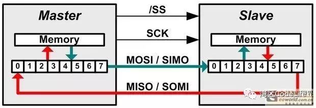
Multi-Master/Slave SPI supports a multi-master/slave structure, but only one master can work at a time because the data transmission clock signal can only be generated by the master (the slave’s signal line SCK is connected to the master’s signal line). In the previous I2C bus, the master finds the slave to communicate through the address information of the slave device. Does the SPI bus distinguish slave devices in the same way? The answer is no. As mentioned, SPI consists of four basic lines, one of which is called chip select line (CS). When the master chooses to communicate with a specific SPI device, it sends a chip select signal (setting the CS signal line to high/low level, depending on the slave’s requirements) to select the slave device, and the selected slave starts working.
-
Data Exchange Here we refer to data exchange, not data transmission, because the SPI protocol stipulates that SPI devices cannot be just “receivers” or “senders”; each clock cycle will send and receive 1 bit of data, which is completed through shift registers, as shown in the figure below: both the master and the slave have a shift register, and they are linked to form a ring (through MOSI/MISO). Accompanied by clock pulses, data shifts from high to low, moving out of the master register and into the slave register, and vice versa. Once all data in the registers has shifted out, the data exchange between the master and slave is complete. One drawback of SPI is that, unlike I2C, it does not have an acknowledgment mechanism, making it impossible to determine whether data has been received.
Four Operating Modes
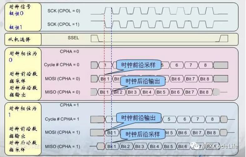
The SPI bus has four operating modes, determined by clock polarity (CPOL) and clock phase (CPHA). CPOL: clock polarity, determines the clock state when the SPI bus is idle; CPOL = 0 means the clock is low when idle; CPOL = 1 means the clock is high when idle. CPHA: clock phase, determines at which clock edge data is sampled; CPHA = 0 means data is sampled at the first clock edge (rising or falling); CPHA = 1 means data is sampled at the second clock edge.
Note: Many people misunderstand clock phase (CPHA), believing that “*When CPHA = 1, the SPI device triggers data sampling on the falling edge of the clock signal and sends data on the rising edge. When CPHA = 0, it is exactly the opposite.” This understanding is clearly incorrect; CPHA does not determine whether data is sampled on the rising or falling edge.
Let’s look at the figure below. When CPHA = 0, data sampling occurs at the first clock edge; when CPHA = 1, data sampling occurs at the second clock edge. However, we can note that with different CPOL values, the first and second clock edges are different (CPOL = 0, the first edge is from low to high, i.e., rising; CPOL = 1, the first edge is falling). Thus, whether data is sampled on the rising or falling edge should be the result of both CPHA and CPOL.
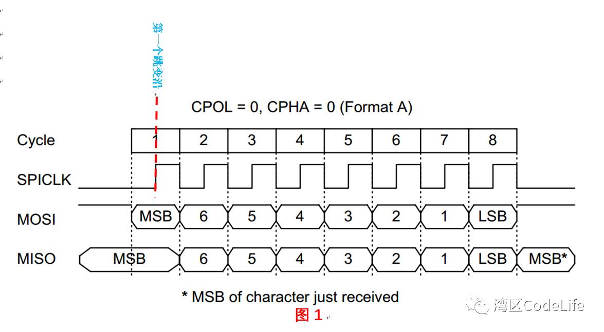
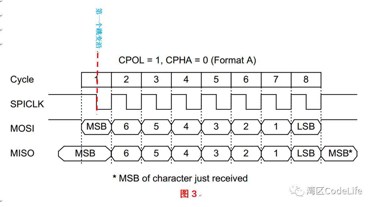
To better understand the four operating modes of the SPI bus, I have extracted four figures from the S3C2440 data sheet to compare the differences. Ignoring the differences between MSB and LSB, in Figure 1, the bus is idle with SPICLK low, and data is sampled at the first clock edge (rising).
In comparison to Figure 1, in Figure 2, the idle state of the bus remains unchanged (because CPOL is the same), but the sampling time has changed; in Figure 2, data is sampled at the second clock edge (falling), and the sampling edge has changed from rising in Figure 1 to falling, but this does not mean CPHA can completely control the edge-triggered signal.
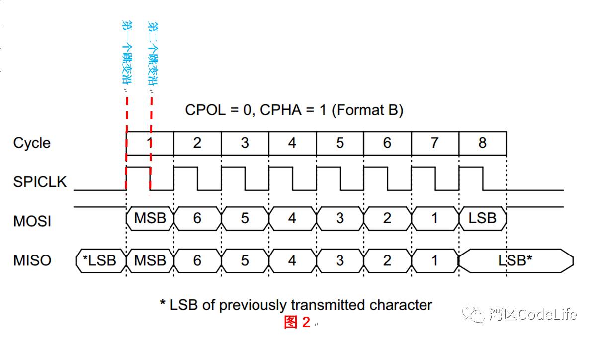
Figure 3 differs from Figure 1 in that when the bus is idle, the clock signal is high, and data is sampled at the first clock edge (falling) (CPHA = 0). Although Figures 1 and 3 have the same clock phase (CPHA), the sampling edges are opposite, further proving that it is incorrect to understand CPHA as controlling the sampling edge.
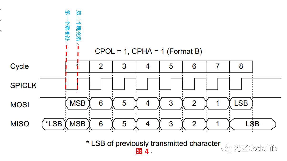
Similarly, comparing Figures 3 and 4, we can further understand that the sampling edge is the result of the interaction between CPOL and CPHA.
It is worth mentioning that the master’s working mode must refer to the slave to determine, because the master’s MOSI connects to the slave’s MISO, and the slave’s MOSI connects to the master’s MISO, so the master’s clock configuration and the slave’s clock configuration should be opposite. When configuring the clock polarity, it is essential to clarify whether the slave device receives data on the rising or falling edge and whether it sends data on the rising or falling edge. For example, the Sychip Wlan8100 Module Spec states: the master sends data on the falling edge of the clock, and the slave receives data on the rising edge. Therefore, the master’s SPI clock polarity should be configured to be effective on the falling edge. The LCD Driver IC SSD1289 also stipulates that the slave SSD1289 receives data on the rising edge of the clock and receives data in order from high to low. Therefore, the master’s SPI clock polarity should also be configured to be effective on the falling edge. Only when the clock polarity and clock phase are configured correctly can data be accurately transmitted between the master and slave devices. Therefore, when configuring the clock, refer to the timing or relevant data sheets of the slave device to configure the master’s clock (since the slave’s clock signal is provided by the master).
Conclusion
This concludes the introduction to the SPI bus. Although the SPI bus requires more pin lines from the master (each slave requires a CS line) and lacks acknowledgment signals, it is favored by many manufacturers due to its support for full duplex, simple operation, and high transmission efficiency. This introduction to the SPI bus ends here; the next article will introduce the powerful UART.