Traditional synchronous digital communication buses rely on two fundamental principles related to signal modulation and maximum likelihood sampling. In short, digital information transmission begins with representing information using data bits, which are then encoded into physical quantities such as voltage potentials or electronic currents. These physical quantities are transmitted through physical media such as metal conductors or free space. Similarly, when receiving data bits, the receiver must quantify the sensed physical quantities and minimize the probability of quantization errors in the presence of noise, attenuation, and interference.
Generalization of Multi-Conductor Transmission Solutions
In digital subsystems such as computers, consumer electronics, or data center servers, the encoding process has traditionally relied almost entirely on two-level Pulse Amplitude Modulation (PAM) schemes, while receiver sampling often employs positive feedback latches (for quantization) combined with synchronous clock signals to achieve maximum likelihood sampling. For example, a logic 1 bit is encoded with a high voltage, while a logic 0 bit is encoded with a low voltage. Since the invention of integrated circuits, this foundational scheme has derived various variants, including using differential voltage signals to achieve electromagnetic interference resistance and ground bounce protection, implementing DC balance and baseline drift protection through digital word encoding, and employing phase-locked loop (PLL)-based forward clock and embedded clock techniques to reduce pin count or lower bit error rates.
Next, we will introduce the MIPI C-PHY interface standard, a new synchronous digital communication bus deployed in high-speed, low-power application scenarios such as smartphones, virtual reality/augmented reality headsets, and Internet of Things devices. The C-PHY standard generalizes multi-conductor transmission solutions, allowing more data bits to be transmitted through a single physical conductor within a unit interval (UI), thus forming a significant difference from traditional digital buses. As shown in Figure 1(a), a typical digital communication link includes differential data buffers for encoding the transmission of digital bits and differential clock buffers for encoding timing synchronization signals. The receiver triggers D flip-flops to sample data bits using the synchronous signal from the clock buffer. This architecture requires four independent conductors (cables) to transmit only 1 bit of data within a single UI.
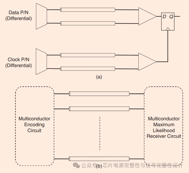
Figure 1: C-PHY Multi-Conductor Transmission Solution (a) A typical digital communication link. (b) A generalized multi-conductor transmission solution.
The C-PHY interface fundamentally addresses the inefficiency of cable count by extending the forward clock differential pair architecture shown in Figure 1(a). Just as differential pairs use two cables to collaboratively encode the physical quantities corresponding to logic bits, the C-PHY standard explores using a set of cables (more than two) to collaboratively encode/transmit more than 1 bit of data per UI. This abstract concept is illustrated in Figure 1(b), referred to as a generalized multi-conductor transmission solution.
In this generalization process, the C-PHY interface adopts innovative methods such as hybrid single-ended/differential signaling schemes and multi-level signal modulation, which are significantly different from traditional two-level differential voltage modulation architectures. Additionally, its multi-phase encoding technology eliminates the need for forward clock transmission, further reducing the number of cables. This article will gradually elaborate on the driving circuit implementation, receiver circuit design, clock recovery mechanisms, and the high-level mapping technology and protocol flexibility of C-PHY, starting from the principles of three-phase encoding.
Three-Phase Encoding
As the first practical application of its underlying multi-phase communication technology, C-PHY implements a three-phase encoding transmission system using three cables. In this system, the three cables work together to create a synchronous data link, achieving a throughput of approximately 2.3 bits/UI. This represents a significant improvement over the 1 bit/UI efficiency of traditional differential data links, while using fewer cables (three instead of four).
Figure 2 shows a circuit diagram of the three-phase encoding C-PHY link. The C-PHY bus has a single-ended structure at the transmitter and a fully differential structure at the receiver. Specifically, the transmitter uses three single-ended phase-matched drivers to modulate the voltage potentials of the transmission medium (three independent cables); the receiver consists of three binary differential amplifiers (the term “three-line group” is used to refer to the channels in C-PHY, similar to the P and N line pairs in differential channels). These amplifiers operate similarly to the traditional differential amplifiers in Figure 1(a), allowing C-PHY to inherit the excellent common-mode noise rejection capabilities of traditional systems.
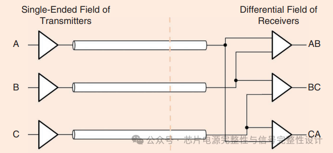
Figure 2: Transmitter and receiver circuits in the three-phase encoding link.
To use conventional binary differential receiving amplifiers, encoding rules must be applied at the transmitter end of the C-PHY link. For example, if the A and B drivers in Figure 2 produce the same voltage potential at the same time, the corresponding differential receiver (AB) will output an uncertain value, determined by its input reference offset voltage, voltage mismatch between the drivers, and the metastable behavior of the differential amplifier/comparator in the receiver. Clearly, the primary encoding rule of C-PHY is that the voltage potentials of the two cables must not be the same within any UI. This rule is achieved by allowing each single-ended driver to generate three-level modulation (rather than the two levels of traditional digital links).
This generalized design using single-ended drivers ensures that the cross-connected differential amplifiers will never see uncertain differential levels. Figure 3 illustrates an example: as time progresses and data is encoded into modulation levels, the voltage potentials of the A, B, and C drivers remain different. In the first UI on the left side of the figure, A is at a high level, B is at a mid-level, and C is at a low level; in the next UI, A switches to mid-level, but B switches to low level, and C switches to high level, ensuring that the voltage potentials of the three cables are always different.
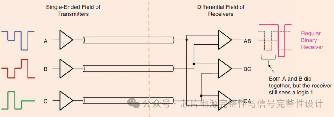
Figure 3: Three-phase single-ended modulation from transmitter to receiver buffer converted to differential binary modulation.
When observed on an oscilloscope, the single-ended driver waveforms are shown in Figure 4. Each cable switches between three different levels, and the same voltage may only occur during the switching period. The instantaneous average voltage of the three cables remains nominally constant, consistent with the characteristic of constant average voltage in differential signals between P and N lines. Furthermore, the transition phases/offsets of the three cables are strictly matched, which is crucial for the normal operation of C-PHY, similar to the phase matching requirements of differential pairs in traditional SerDes links.
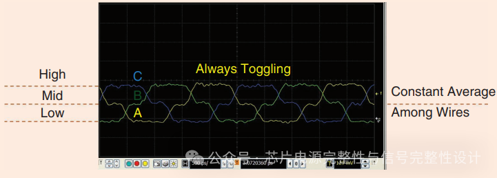
Figure 4: Signal waveforms observed at the transmitter
Observing the differential amplifier waveforms on the right side of Figure 3 leads to a key conclusion: although the input cables of each pair of differential amplifiers may simultaneously drop (as shown by the AB amplifier), their difference is always a finite positive or negative value. In the few UIs shown in the figure, the A and B lines frequently switch, but the quantized differential waveform (thick magenta) only experiences a transition when its difference changes from positive to negative.
When observed on an oscilloscope, the input waveforms of the C-PHY differential receiver are shown in Figure 5. This figure illustrates the AB receiver waveforms corresponding to the pattern in Figure 4. The three levels of the single-ended cables convert into four levels in the differential waveform, representing weak and strong versions of logic 0 and logic 1. Ultimately, the binary differential receiver only recognizes logic 0 or logic 1. The weak and strong versions of logic 0/1 are products of the three-level encoding (see the “Note” regarding the discussion of multi-level waveforms in C-PHY).
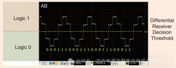
Figure 5: Signal waveforms seen by the receiver
Driving Circuit Implementation
As a high-speed communication link, C-PHY must drive long transmission lines (i.e., signal propagation delay exceeds rise time), so the driver design must consider impedance matching and equalization. At the same time, the C-PHY link is optimized for ultra-low power applications, and circuit implementations typically use voltage mode drivers rather than current mode drivers. The industry consensus is that voltage mode drivers generally have advantages in low power consumption and small size.
The single-ended structure of the differential voltage mode driver consists of a pair of transistors, a pair of termination resistors, and a voltage supply rail (Figure 6(a)). The figure shows a simple NMOS implementation, but any voltage mode implementation (whether NMOS or CMOS) is applicable. Similarly, the construction of the termination resistors is not restricted; it is only necessary to emphasize the functional behavior of the driver and how it translates into a C-PHY driver. Specifically, in a differential voltage mode driver, the pull-up and pull-down transistors drive in a complementary manner: if the positive side half driver of the differential pair is pulled up by the data bit, the negative side half driver is pulled down by the same data bit; simultaneously, the positive side is pulled down by the complement of the data bit, and the negative side is pulled up by the complement. This configuration produces truly balanced complementary differential pair behavior: when P outputs a high level, N simultaneously outputs a low level. A single pre-driver must generate a single data bit and its complement. The C-PHY pre-driver sends two independent bits to the voltage mode buffer (Figure 6(b)). These two bits can encode high, low, or mid-levels; apart from this, the C-PHY driver has the same single-ended structure as the differential driver.
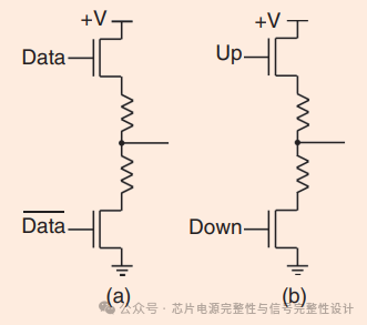
Figure 6: (a) Differential voltage mode driver (b) Three-phase encoding transistors
However, the mid-level driving presents a special challenge in C-PHY: whether the voltage mode driver needs to actively drive the mid-level (forcing the cable potential) or let the cable float. From a first-order analysis, there is no need to actively drive the mid-level; it is sufficient to let the cable float (disconnecting the pull-up and pull-down transistors of the driver). The reason is that C-PHY requires the receiving end to perform termination matching on the transmission line to minimize reflections, and the termination at the receiving end ensures the generation of the mid-level. More precisely, the cable encoding mechanism described earlier guarantees that when the pull-up and pull-down transistors of the floating driver are off, the cable will be at an intermediate potential generated by the termination resistors (RL) of the A and B lines. However, floating pull-up and pull-down transistors cannot provide adequate reverse termination matching, which may lead to severe echo loss in actual systems. Therefore, in high-speed applications, actively driving the mid-level is always preferable.
Explanation of Termination and Signal Routing
As mentioned earlier, the cable encoding mechanism of C-PHY ensures that the average levels of the three cables remain constant, but the circuit implementation principles or why the driver is allowed to float at mid-level have not been explained. This section elaborates on this topic through Figure 7. Figure 7(a) shows that when line A is pulled high and line B is pulled low, this line pair can be assumed to operate as a conventional differential pair. If each cable is terminated with a floating load resistor (RL) equal to the characteristic impedance of the transmission line and the source impedance of the driver, the midpoint between the two cable termination resistors can be observed to stabilize to the common-mode voltage (nominally +V/2) of the two cables. This midpoint is referred to as the common point of the three-line group. Regardless of whether the pull-up and pull-down transistors of line C are driving the mid-level, as long as the transistor and resistor parameters nominally match, there will be no DC current flowing through the cables.
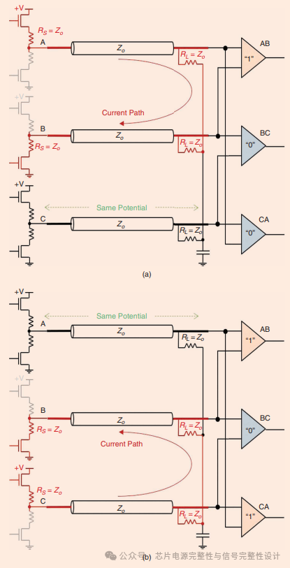
Figure 7: Load circuit at the end of the transmission line, (a) A pulled high, B pulled low, C at mid-level, (b) A at mid-level, B pulled low, C pulled high, how the signal levels average to a constant value in a DC sense.
Specifically, if the pull-up and pull-down transistors are floating, there is no DC path on the driver side, and the cable potential will be pulled to the intermediate potential by the termination resistors RL of lines A and B. Similarly, if the pull-up and pull-down transistors are driven to mid-level, this potential will equal the potential set by the RL resistors of lines A and B, resulting in no DC current under first-order approximation. From a DC perspective, the termination at the common point is consistent with the three-phase encoding scheme that maintains constant average voltage across the three-line group. Figure 7(b) illustrates the driving scenario when line B is pulled low and line C is pulled high, which can be verified similarly.
Regarding AC termination, as mentioned earlier, C-PHY must drive long transmission lines, so electromagnetic wave propagation theory must be applied. Each single-ended driver’s switching event propagates electromagnetic waves along the transmission line, and its AC termination (reflection suppression) must be achieved by adding decoupling/termination capacitors at the common point. This capacitor provides a virtual AC ground for the incident wave, absorbing energy and preventing it from reflecting back to the source through the three-line group.
Since each driver sends independent edges and the transmission lines are typically routed in a non-coupled manner, this termination scheme is equivalent to a single-ended communication link. Edges are generated when the driver switches any level (low, mid, high), so the amplitudes of the edges on the C-PHY transmission line may not be equal (e.g., low→mid and low→high).
Self-Clocking and Clock Recovery
Earlier, the C-PHY signal transmission and transmission line termination circuits were introduced. Regarding the receiver, only the buffer design equivalent to traditional differential pair receiving amplifiers was described. This section will elaborate on the synchronization mechanism between the transmitter and receiver circuits, detailing the receiving path and clock recovery structure.
The second key signal rule of C-PHY enables clock recovery, which is heuristically described in Figure 8. In short, the C-PHY encoder ensures that at least one receiving amplifier detects a transition within each clock cycle, even if individual cables remain stable for an extended period. For example, in Figure 8, line B may remain constant, but C-PHY requires the complementary cables to be at different levels, and at least one transition must occur within each UI, so at least one receiver will detect an edge in each UI (right side of Figure 8). All receivers in the figure show edges in each UI, but this is merely a special case of the left-side condition. Generally, only one differential amplifier needs to generate an edge in each UI.
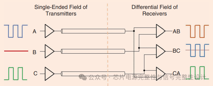
Figure 8: Signal waveforms with a constant value on one of the conductors
This transition requirement allows C-PHY to achieve clock recovery without complex or high-power phase-locked loops. The link achieves self-clocking through forced transitions at the UI boundaries, and the receiver utilizes these transitions to recover the clock. Meanwhile, the recovered clock and data sampling circuits must respond immediately to transitions in the data stream, employing negative hold time sampling techniques.
Figure 9 illustrates the functional schematic of the clock data recovery circuit in C-PHY. Each amplifier may or may not produce edges, but all are equipped with edge detection circuits. The first of the three edge detection outputs is selected as the sampling clock for the current UI, driving conventional D flip-flops. It should be noted that the edge detection function must be carefully designed. The edge detector will inevitably include finite delays, which will limit the minimum eye diagram width that can be sampled. If the delay is too long, it may lead to the edge detector and subsequent clock gating unit sampling the wrong eye diagram. This could be one of the biggest challenges for the large-scale deployment of C-PHY in cost-sensitive applications.
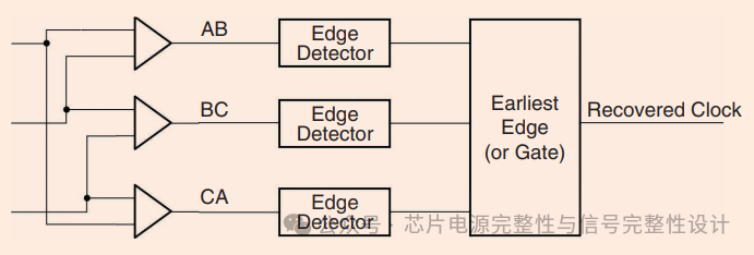
Figure 9: Clock recovery circuit in C-PHY
C-PHY Word Mapping
Without delving into the C-PHY protocol layer, it is beneficial to understand how the multi-bit symbols transmitted by the three-line group in each UI are converted into digital data usable downstream or upstream. To this end, the cable states are defined as the level combinations of lines A, B, and C. The earlier rule (no two cable levels can be the same within any UI) implies that there are only six unique cable states. Similarly, the rule that cable state transitions must occur in each UI means that the current cable state must switch to one of the other five states. Symbols are defined as transitions between cable states, so each UI encodes one of five possible symbols. Figure 10 summarizes these concepts. The orange panel (second to last layer) represents data transmission, showing that data is only transmitted during state transitions. Data is transmitted as symbols rather than bits, as a single symbol encodes more than 1 bit of information (similar to how a single symbol in PAM4 represents 2 bits).
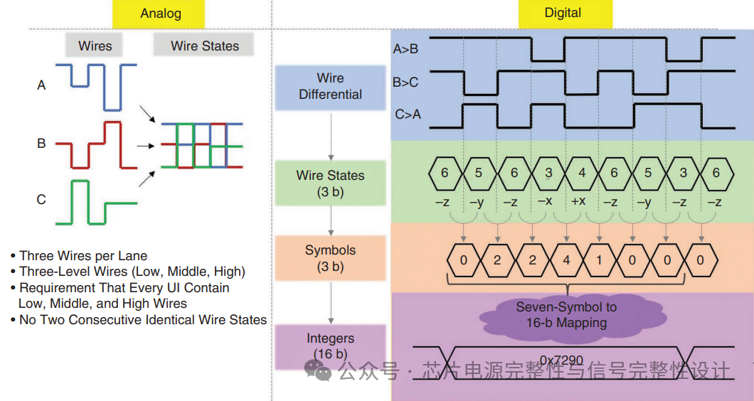
Figure 10: Summary of C-PHY data types. Cable states are represented by numbers 1 to 6; symbols are transitions between states, with five possible symbol values per UI; the space of seven unique symbols exceeds the space of 16b, allowing for a complete representation of a 16b word.
The mapping task is to convert symbols into digital words. To this end, C-PHY adopts a word mapping paradigm: every seven symbols map to a unique 16-bit digital word. This means that the number of words that C-PHY can transmit is 5^7=78,125, while a 16-bit word contains 65,536 combinations, so seven symbols can fully represent a 16-bit word. The bottom panel of Figure 10 illustrates the principle of mapping a 16-bit word to seven symbols. In practical implementation, this is essentially a one-to-one mapping of 65,536 numbers, so each symbol encodes approximately 2.3 (16/7) bits of information.
C-PHY has a large number of unmapped seven-symbol combinations (78,125-65,536=12,589), which provides unique opportunities for the protocol layer. For example, traditional SerDes links require alignment markers to define word and packet boundaries due to timing uncertainties, while C-PHY can achieve unambiguous alignment by sending unmapped seven-symbol words (such as SYNC header 3444443) (Figure 11). Such unmapped words do not represent any 16-bit numbers and can be sent at any time in the data stream.
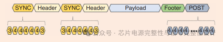
Figure 11: Unmapped symbol sequences can be used to transmit sideband messages over the same line
Unmapped words further support the transmission of sideband signals over the same set of cables. Traditional protocols often rely on additional buses such as I2C or SPI for control or interrupt handling, which increases pin count. The unmapped words of C-PHY allow sideband messages to be sent without affecting the main data packet transmission, and some low-power mobile applications have already utilized this feature to reduce additional pin requirements.
Conclusion
This article introduces the C-PHY signal standard—a new multi-conductor solution that supports approximately 2.3 bits/UI of information through multi-level signals, achieving high data bandwidth efficiency in constrained transmission channels. The concepts of three-phase encoding, circuit implementation techniques, clock recovery mechanisms, and high-level mapping requirements (including the use of unmapped words for sideband signaling) have been detailed. C-PHY represents a new type of digital bus that breaks through traditional signaling modes by combining the advantages of single-ended and differential signals, maintaining low pin counts while not sacrificing electromagnetic noise immunity.