If you want to engage in camera driver software development, what basic information do you need to prepare? This article summarizes it.
From an independent component perspective, it includes two parts: the sensor module and the core board; thus, the core of the driver software is to ensure the connection between the two. The common hardware interfaces are MIPI and USB, with a focus on the PHY layer during MIPI interface debugging; the common software driver frameworks are V4L2 and UVC.
There is too much content; this chapter summarizes MIPI camera and USB camera, and another article will follow.
The camera sensor module serves as the image input, providing the data source;
The core board receives and processes the module’s input for processing and display;
The hardware interface provides a physical connection method, and the camera driver software drives the soft connection between the two, generally utilizing some mature software driver frameworks.
00 Common Basic Concepts
Video input technology refers to the technology that transfers real images captured through optical-electronic technology to a storage medium via a camera.
The camera module, as a video input device, physically captures images and is widely used in various fields such as real-time monitoring, automotive applications, and video recording.
A local camera refers to the integrated camera used in this article.
A network camera can connect directly to the network; it connects to portable network devices using video codecs and then transmits images back to human-machine interaction terminals via the network.
MIPI (Mobile Industry Processor Interface) defines a series of interface standards for internal connections in mobile devices. The MIPI interface defines four pairs of differential signals for transmitting image data and one pair of differential clock signals, initially established to reduce the number of connections between the LCD and the main control chip (replacing parallel interfaces), ultimately supporting high-definition displays and cameras.
Taking the RK3399 chip platform as an example, it integrates three MIPI interfaces: DPHY0 (TX0), DPHY1 (TX1RX1), and DPHY2 (RX0), where TX can only send data, and RX can only receive data to ISP0. There are two PHYs, each supporting 1 lane, 2 lanes, or 4 lanes, with a maximum support of 13M pixel raw sensors.
01 Sensor Interface
The camera sensor driver interface consists of two aspects: (1) Sending and receiving control commands and configuration parameters through the IIC interface to initialize the sensor and configure its parameters (such as resolution, frame rate, exposure, etc.); (2) Correctly transmitting and parsing image data through the MIPI interface.
IIC bus: Two signal lines (SCL clock line and SDA data line), the camera sensor usually acts as a slave device, with the master device (such as the processor) completing the configuration and control of the slave device through the IIC interface.
IIC function: Through the IIC interface, the master device can send control commands and configuration parameters to the camera sensor, such as setting image resolution, exposure time, white balance, etc.
MIPI interface: Uses differential signal transmission technology, effectively reducing signal interference and power consumption, and is a high-performance, low-power serial communication interface.
MIPI function: Supports various data encoding formats (such as YUV, RGB, RAW, etc.) and different data widths (such as 8-bit, 10-bit, 12-bit, etc.) for image data transmission of camera sensors. Additionally, some advanced features like phase detection autofocus and HDR also need to be implemented through the MIPI interface.
Other power supply and clock interfaces are connected according to hardware connections.
02 MIPI Interface Parameters
Below are some examples of commonly used MIPI parameters (for reference only, as different hardware platforms and standards may vary):
| Parameter Name | Example Specifications | Description |
|---|---|---|
| Data Rate | 1.5 Gbps / 3 Gbps / 6 Gbps | The supported data transmission rate range, depending on the hardware platform and standard |
| Lane Count | 2 Lane / 4 Lane | The number of supported MIPI lanes; increasing the number of lanes can improve data transmission rates |
| Clock Frequency | 100 MHz / 200 MHz | The clock signal frequency driving the MIPI interface, affecting data transmission rate and stability |
| Rise/Fall Time | < 100 ps | The rise and fall times of MIPI signals, affecting signal integrity |
| Eye Diagram Opening | > 80% @ 1 Gbps | A key indicator for assessing signal integrity, affecting the reliability and stability of data transmission |
Parameter Description:
 (1) Data Rate refers to the speed of data transmission through the MIPI interface, measured in Gbps (Gigabits per second).
Different MIPI standards and hardware platforms support different data rate ranges. Increasing the MIPI rate can accelerate data transmission speed, allowing more image data to be transmitted in the same time, thus increasing the bitstream. However, low-power or low-cost solutions may support lower data rates.
During debugging, it is necessary to select an appropriate data rate based on system requirements and camera performance, and set it through driver configuration. Use debugging tools (such as oscilloscopes, logic analyzers) to monitor the waveform and timing of MIPI signals, ensuring that the adjusted rate is within the hardware-supported range and that the signal quality is good.
 (2) Lane Count refers to the number of MIPI lanes used for data transmission. Each lane can independently transmit data, so increasing the lane count can improve the total data transmission rate.
Common lane counts are 1, 2, 4, etc. The maximum lane count supported by different cameras and processors may vary. During debugging, it is necessary to select an appropriate lane count based on the system’s data bandwidth requirements and hardware support.
(3) Clock Frequency refers to the frequency of the clock signal used to drive the MIPI interface. The clock frequency directly affects the data transmission rate and stability.
The specifications of the clock frequency depend on the MIPI standard and hardware design used. Engineers need to set an appropriate clock frequency based on system requirements and hardware specifications.
During debugging, it is necessary to ensure the stability and accuracy of the clock signal to avoid data transmission errors or delays.
(4) Signal integrity parameters, including rise time, fall time, eye diagram opening, etc., directly affect the transmission quality and stability of MIPI signals.
The specifications of signal integrity parameters are usually determined based on the quality of the transmission line used, the performance of the signal driver and receiver, and the electrical characteristics of the system.
During debugging, it is necessary to use tools such as oscilloscopes and logic analyzers to monitor and analyze the waveform and timing of MIPI signals to ensure that signal integrity meets the requirements.
(5) Summary. After modifying MIPI parameters, it is necessary to apply for a corresponding specification of sensor settings from the sensor manufacturer to ensure that the camera can operate normally and output image data that meets the requirements.
The specifications of the clock frequency depend on the MIPI standard and hardware design used. Engineers need to set an appropriate clock frequency based on system requirements and hardware specifications.
For example, adjusting the MIPI rate is actually adjusting the clock frequency for data transmission. Therefore, it is necessary to adjust the internal clock divider of the sensor to ensure that the sensor’s clock configuration matches the new rate.
After modifying the lane count, it is necessary to ensure data synchronization between the various lanes during multi-lane transmission. Therefore, a common clock signal and synchronization signal are required, which may necessitate adjustments to the sensor’s synchronization mechanism.
03 MIPI – CSI Hardware Interface
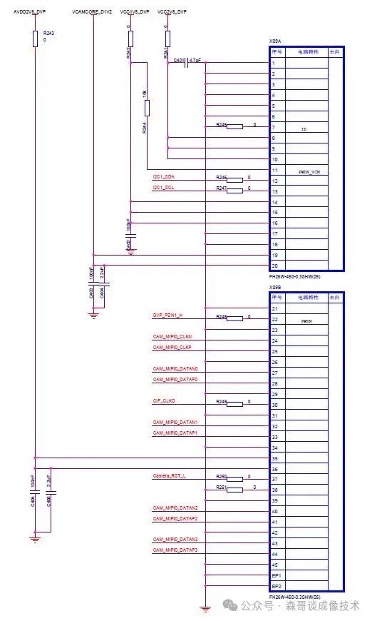
The camera module uses the V13850 module as an example, with hardware utilizing the MIPI CSI interface, and the software on the Android platform completes the driver and configuration of the OV13850 module at the hardware abstraction layer.
The camera control uses the MIPI-CSI mode, which includes not only the MIPI interface but also three power supplies, I2C, MCLK, and GPIO pins.
The three power supplies used include VDDIO (IO power consistent with the MIPI signal line voltage), AVDD (analog power 2.8V or 3.3V), and DVDD (digital power 1.5V or higher).
GPIO mainly includes power enable pins, PowerDown pins, reset pins, etc. The schematic is as follows:
04 MIPI PHY Physical Layer
01
MIPI Protocol Architecture
The overall architecture of the MIPI interface includes the physical layer, protocol layer, and application layer.
The application layer provides data to the protocol layer and specifies the data transmission requirements and rules;
The protocol layer encapsulates the data into a format suitable for transmission based on these requirements and rules, providing a framework and rules for data transmission to the physical layer;
The physical layer (PHY) is responsible for sending the encapsulated data from the protocol layer through the physical medium. The PHY layer is directly connected to the physical medium and is responsible for converting physical signals to digital signals, ensuring that data can be transmitted correctly and efficiently through the physical medium.
02 MIPI PHY
The focus on the PHY during MIPI interface debugging is due to:
(1) The PHY layer is the foundation of data transmission, directly involving physical connections, thus directly affecting transmission quality.
(2) The PHY layer has complexity; the MIPI standard defines various PHY layer specifications suitable for different scenarios, and the technical details involved in the PHY layer are very rich, including differential signal transmission, clock recovery, data encoding and decoding, etc.
(3) The PHY layer offers convenience for debugging and quick problem localization; tools such as oscilloscopes and logic analyzers can be used to directly observe and measure signal waveforms, timing, and levels.
03 Types of MIPI PHY
| Type | Lanes | Working Mode and Features | Main Applications |
|---|---|---|---|
| C-PHY | Each lane contains three differential data lines | Has extremely high transmission rates | Image acquisition devices |
| D-PHY | Each lane typically consists of a pair of differential lines | Supports both high-speed and low-power modes | Display devices |
| Combo-PHY | Combines the features of C-PHY and D-PHY | Combo-PHY can switch between C-PHY and D-PHY modes for flexible data transmission. |
05 Software Driver Architecture V4L2
01
Driver Software Code
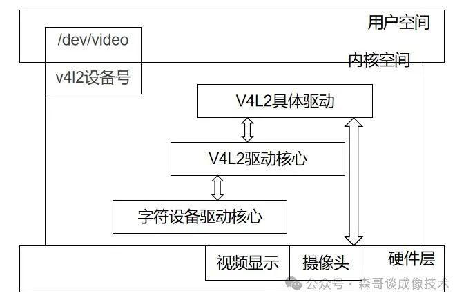
V4L2 (Video4Linux2) is a general API for video devices in the Linux kernel, supporting video capture, streaming playback, video output, etc.
V4L2 supports three types of devices: video input/output devices, VBI devices, and radio devices, among which the most widely used video input device in V4L2 is the camera input device.
The core source directory of V4L2 is /kernel/drivers/media/v4l2-core/.
The core of the V4L2 driver, v4l2_dev.c, includes the registration of the main structure video_device, creating device nodes like video in the /dev directory.
Key structures in V4L2 include v4l2_device, v4l2_subdev, video_device, etc.
Common ioctl commands in V4L2 include VIDIOC_QUERYCAP, VIDIOC_S_FMT, etc.
The core process of the driver code:
(1) Initialize the V4L2 device and register the device node (e.g., <span>/dev/video0</span>).
(2) Register the camera sub-device, such as the ISP sensor device.
(3) Query the device’s supported features using <span>VIDIOC_QUERYCAP</span>;
(4) Set the image resolution, pixel format, etc., using <span>VIDIOC_S_FMT</span>;
(5) Request buffers using <span>VIDIOC_REQBUFS</span> and map the buffers to user space using <span>mmap</span>;
(6) Control the start and stop of video streams using <span>VIDIOC_STREAMON</span> and <span>VIDIOC_STREAMOFF</span>.
02 V4L2 Architecture Framework
-
V4L2 Core Driver Framework: The core part of the V4L2 framework is mainly responsible for constructing the standard video device driver framework in the kernel and providing unified interface functions. It includes functions for registering, unregistering, and querying video devices, as well as interaction interfaces with sub-devices.
-
V4L2 Lower Layer Interface Driver Framework: Responsible for connecting specific video devices (such as camera sensors) to the V4L2 framework. It includes hardware-related interface implementations, such as I2C, SPI, and the interaction logic with sub-devices like sensors.
-
Sub-device Specific Drivers: Sub-device drivers (such as sensor drivers, ISP drivers, etc.) interact with the main device through the interfaces provided by V4L2. They implement specific hardware control logic, such as sensor initialization and image data acquisition.
-
Character Device Interface: In Linux, all peripherals are treated as files. The V4L2 framework provides access to video devices in user space through character device interfaces (such as /dev/videoX). User space applications can access video devices through standard file operation interfaces (such as open, read, write, ioctl, etc.).
-
Video Buffer Management: The V4L2 framework provides a management mechanism for video buffers, facilitating efficient transmission of video data between kernel space and user space. This is typically implemented through modules like videobuf2.
Summarizing and organizing always takes time; the entire writing process has spanned too long. Please give a thumbs up and follow to encourage!