A common misconception is that pull-up resistors are always required on SPI bus lines. I want to make it clear that pull-up resistors are not always necessary for the basic function of sending and receiving digital data on the SPI bus.
The buffers in the SPI interface use a push-pull topology, which involves high-side and low-side switching MOSFETs, essentially forming a CMOS inverter. As we will see in this article, the presence of pull-up resistors does not affect the basic switching functionality of the push-pull bus.
That said, in certain cases, it is reasonable to place pull-up resistors on a push-pull bus, and some component manufacturers recommend or require this in certain datasheets. We will explore these cases and their impact on system behavior. While there can be more complex solutions to eliminate the need for pull-up resistors in these situations, placing pull-up resistors can simplify design and ensure proper interface operation.
How Pull-Up Resistors Work with SPI Bus
Let’s take a look at a typical model of the buffers in the SPI interface. All SPI buffers use a push-pull topology, which consists of high-side and low-side switches to drive signals onto the bus, and each signal on the SPI bus (CS, MOSI, MISO, and SCLK) employs this topology. The diagram below shows an example of this circuit. It is important to note that real SPI buffers are not as simple as two MOSFETs, but the same principle applies in general.
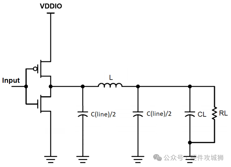
CMOS inverter as an SPI driver. The output is connected to the traces (represented as lumped components) and the load circuit (RC equivalent model).
The reason for using this topology is that the discharge capacitance in the buffer circuit can provide a relatively fast edge rate at the output, which will be much shorter than the clock period on the bus. This allows for data rates that are faster than open-drain protocols (such asI2C).
The SPI bus with pull-up resistors essentially acts as a CMOS inverter driver, where the high-side FET in the output buffer is in parallel with a resistor. Now, let’s examine what happens in each switching state of the driver and what occurs on the bus.
Logic High Output
In the logic high output state, the NMOS is off, and the PMOS is on. At this point, VDDIO provides current to the connected traces and load. The capacitance in the traces and load then begins to charge until the voltage across the load matches VDDIO. At this time, the on-resistance of the PMOS is approximately milliohms, while the pull-up resistor is about 1 to 10 kOhms. Clearly, the pull-up resistor is so large that in the logic high output state, it is effectively shorted by the PMOS.
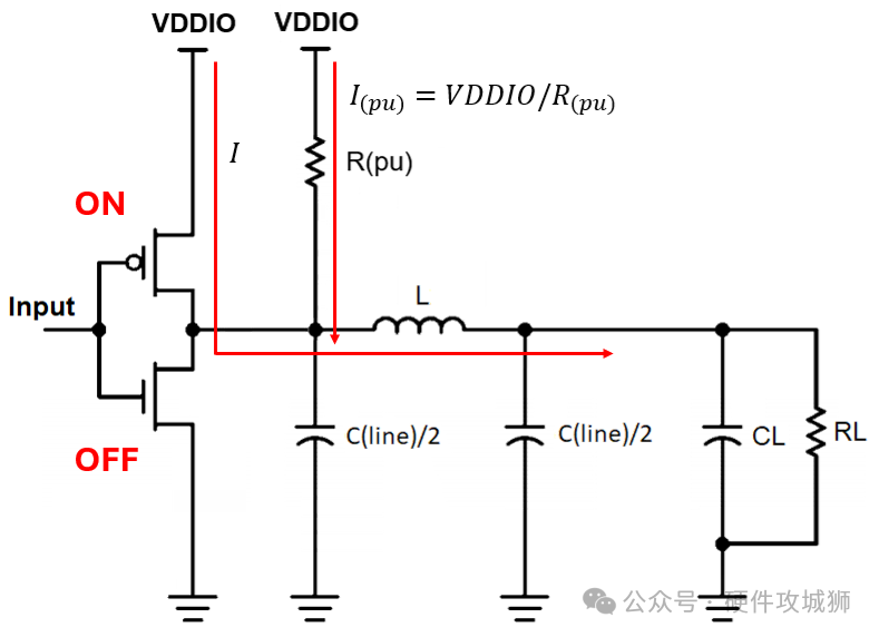
Since all current flows through the PMOS in the high logic state, the switching characteristics are unaffected regardless of the presence of the pull-up resistor.
Logic Low Output
Now assume the circuit has switched to the logic low output state. In this state, the NMOS is on, and the PMOS is off, so the traces and load capacitance discharge through the NMOS to the GND network. Since the PMOS is off, it presents a very high resistance (in the MOhm range), much greater than the value of the pull-up resistor (1 to 10 kOhm).
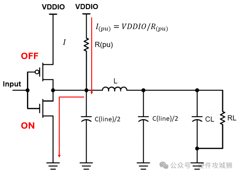
Because the pull-up resistor is relatively small in this case, it allows current to flow through the NMOS for VDDIO/R(pu). For a pull-up resistor of 1 to 10 kOhm, with VDDIO = 3.3 V, the leakage current into the NMOS will be 0.33 to 3.3 mA. This is far less than the typical current of SPI (about 50 mA), so we will not notice any impact on the switching characteristics. The fall time on the bus will be limited by the load and trace capacitance, the output resistance impedance of the buffer circuit, and the on-resistance of the NMOS.
If Switching is Unaffected, Why Use Pull-Up Resistors?
Clearly, placing pull-up resistors on SPI lines does not affect their ability to drive signals onto the bus. Therefore, pull-up resistors should serve other functions unrelated to data transmission; otherwise, they would not be used.
The reasons for using pull-up resistors on one or more lines of the SPI interface depend on specific circumstances. Situations where pull-up resistors are used include:
- Placement on the CS line of peripherals
- Placement on the MISO line of the host device
- Placement on the MOSI line of peripherals
- Placement on all buses near output pins
The rationale for placing pull-up resistors in any of the above cases is to set the logic state of a specific peripheral component on the bus. The most common recommendation is to place a pull-up resistor on the CS pin of a peripheral to pull it high. If the peripheral has a low-active enable pin, that pin will always be pulled high unless the driver side of the pull-up resistor sets it low.
Below is an example of such usage. In PCB layout, pull-up resistors should be placed close to the CS pin of that peripheral.
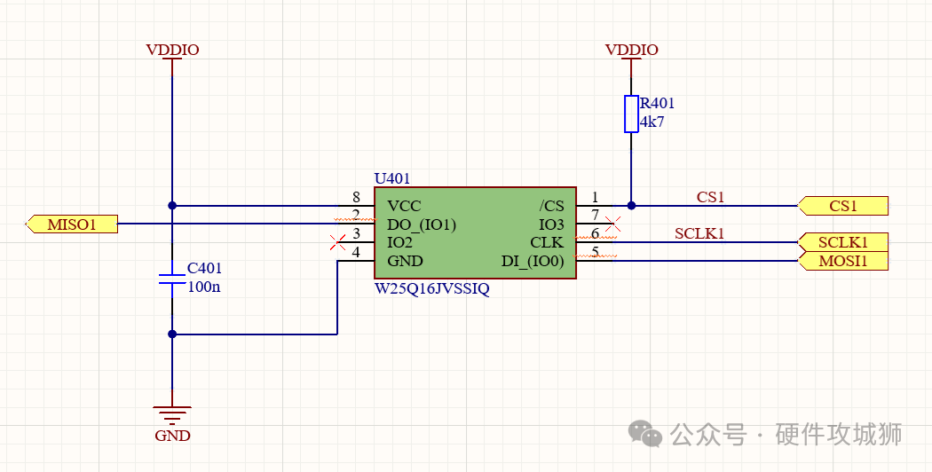
Typical placement of pull-up resistors on the CS pin of the SPI bus.
Why use this pin? The official explanation is that during system startup, the CS pin may float in any state, which can lead to noise corrupting data on the bus. Additionally, if the host device starts before the peripheral and the CS pin is inadvertently enabled, the host may begin operating on data in the peripheral. Sometimes, this is considered the reason for placing pull-up resistors on memory peripherals.
So far, I have not found a compelling reason to place pull-up resistors on the SCLK (clock) line (unless explicitly stated in the datasheet). The reason is that regardless of the presence of the clock signal, if other conditions (especially the CS line state) are not met, the receiving logic circuit will not switch. Some application notes and datasheets recommend using pull-up resistors on MISO or MOSI for various reasons, but testing their effectiveness is straightforward, and the resistors can be desoldered at any time during prototyping.
Follow the Datasheet
If your component datasheet explicitly states that a pull-up resistor is required on a specific SPI pin, you should follow this recommendation. This advice is based on the intent of the chip design engineers and is often used in cases of multifunction pins and/or to set pin states when the pin is disconnected. This is not a PCB layout guideline but a simple circuit functionality guideline: if the datasheet requires a pull-up resistor, then you should place it.
Conversely: SPI lines can operate normally without placing pull-up resistors. If the datasheet does not explicitly mention placing a pull-up resistor on a certain SPI pin, then the normal operation of that pin/interface is not strictlyrequired. In this case, consider the situations mentioned above and whether they apply to your specific system.
Article translated from:altium— End —
The statements and views expressed in this account remain neutral regarding all original and reprinted articles, and the articles pushed are for readers’ learning and communication purposes only. The copyright of the articles, images, etc., belongs to the original authors. If there is any infringement, please contact us for deletion.
Recommended Reading:Share a current detection, sampling resistor Rshunt range switching circuitWhy is it often required for MOSFETs to turn off quickly, but not to turn on quickly?High-speed interface layout guidelinesBuying an oscilloscope for 3 million, let’s take a look inside! (I really opened my eyes)