Hello, everyone. Last time we introduced the substrate in packaging, and this time we will discuss the processes involved in substrate manufacturing.
After processing, the substrate mainly consists of two materials when viewed in cross-section — dielectric and metal. In terms of metal, the majority is copper, while solder joints are used for connections. In lead-free processing environments, SAC (Tin/Silver/Copper) solder dominates.
Unlike the singularity of metal materials, the selection of dielectrics is more diverse. The two most commonly used types are different forms of epoxy resins, both of which are thermosetting types.
FR-4 (also written as FR4) is currently the most well-known resin material in the field of printed circuit boards (PCBs). Here, “FR” stands for “Flame-Retardant,” and “4” is the designation assigned by the National Electrical Manufacturers Association (NEMA) in the United States. It is a composite material made from glass fiber cloth impregnated with epoxy resin.
For higher performance, BT epoxy resin (bismaleimide triazine) can be selected. Its high-temperature resistance is superior, which can be measured by the “glass transition temperature (Tg)” — the temperature at which the resin begins to melt and lose structural integrity. Additionally, BT epoxy resin has a lower dielectric constant, which helps reduce inter-layer signal crosstalk.
Both of the above materials are available in the form of “prepreg” products, which is short for “pre-impregnated.” The manufacturing process of prepreg involves impregnating fiber substrates (usually in cloth form) with resin and partially curing them to stabilize their form. This prepreg can be directly used as a convenient lamination material, and once all layers are in place, complete curing is performed. After all layers are laid out, heat and pressure are applied to achieve full curing and tight bonding of all layers.
Ajinomoto has introduced a newer material — ABF (Ajinomoto Build-up Film). This material offers improvements in dielectric and thermal performance, making it suitable for high-performance signal transmission scenarios. ABF is typically supplied in roll form, with a protective film on both sides: one side is an OPP film, which is removed before use; the other side is a PET film, which is removed after laying. Some ABF dielectric films may also be pre-coated with a layer of copper foil.
In addition to having a lower dielectric constant, ABF’s coefficient of thermal expansion (CTE) is closer to that of copper and other materials on the substrate. Therefore, the likelihood of cracking and other defects during repeated thermal cycling is lower, which is particularly important for packaging circuits that require high reliability. However, its cost is higher than that of traditional simple materials and processes.
It is important to note that the entire substrate does not have to use the same dielectric. Depending on the signal requirements of each layer, different types of resin can be selected for different laminations.
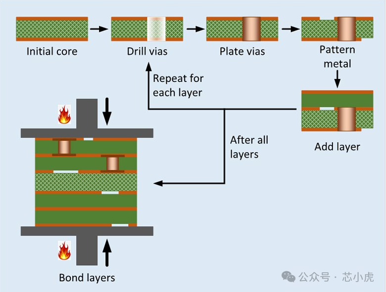
Substrate Manufacturing Process
The manufacturing steps for the substrate are quite straightforward — starting with a core layer, materials are added layer by layer, while simultaneously creating circuit patterns and drilling holes. Buried vias and micro vias can be made in any layer, blind vias must be made in the outer layers, while through vias are drilled after all layers have been laid. The detailed manufacturing process is as follows:
1. Start with a core layer that is metallized on both sides (usually copper-clad).
2. Drilling and plating of vias:
a. Use mechanical drilling or laser drilling to process the hole locations.
b. Perform decontamination and clean the hole walls.
c. Deposit a copper seed layer (to provide a conductive substrate for subsequent plating).
d. Plate the hole walls and surfaces (to form a conductive layer).
3. Patterning the metal layer (creating circuits):
a. Apply photoresist to the surface of the metal layer.
b. Transfer the circuit pattern onto the photoresist through photolithography exposure.
c. Remove the developed photoresist (exposing the metal areas to be etched).
d. Etch the exposed copper layer (to form the desired circuit pattern).
e. Remove all remaining photoresist and clean the surface of the substrate.
4. If more layers are needed, add new resin and copper layers.
5. Repeat steps 2 (via processing) and 3 (patterning) until all layers are completed.
6. Apply pressure and heat to laminate all layers together.
The above steps and materials are aimed at the most common type of substrate. In actual production, the core layer can also use other materials, such as ceramics or metals; additionally, other special-purpose resins may be selected based on requirements. When choosing substrate materials, a comprehensive trade-off must be made between cost, reliability, thermal management capability, signal integrity, and power integrity based on specific application needs.
If you have any comments or suggestions, feel free to leave a message or send a private message. If there are any inaccuracies, please point them out; I am also learning and growing.

*Disclaimer:This article is created by the original author.The content of the article represents their personal views, and our reposting is for sharing and discussion only, not representing our endorsement or agreement. If there are any disputes or infringements, please contact us for removal!Source: semiengineering
▌⊰Related Knowledge Navigation ⊱
What is Q-Time in Smart Manufacturing?
How to Understand Process Flow in Semiconductor Smart Manufacturing
Important Process in Chip Manufacturing – Back Grinding
What Stages Must a Semiconductor Chip Manufacturing FAB Go Through to Achieve Full Automation?
In Batch Operations, When Does a Semiconductor FAB Use Lot? When Does It Use Batch?
▌Click below to follow “Chip Little Tiger” ↓,click the upper right corner to set as a star,to share more chip knowledge and news
▌If you like it, please “like” + “look at” ✿, thank you
▌For learning, communication, and collaboration, please scan the following to add, and note your name + position + company, thank you!

▌Semiconductor Industry Information Database, dedicated to those in need, thank you!