In today’s world where smart devices are ubiquitous, Printed Circuit Boards (PCBs) serve as the “skeleton” and “lifeblood” of electronic products, silently carrying the flow of current and the transmission of signals. Whether it’s a smartphone, computer, or smart home device, the realization of core functions is inseparable from the precise layout of PCBs.
1. Getting to Know PCBs: The “Skeleton” and “Lifeblood” of Electronic Products
PCB (Printed Circuit Board) is the most basic and crucial component in electronic devices. Imagine when we open a smartphone or computer, we see a green board covered with lines and components—this is the PCB. It is like the road system of a city, connecting various electronic components (like buildings) through copper foil wires (equivalent to roads), providing a transmission channel for current.
The basic structure of a PCB consists of four layers:
-
Substrate Layer (Insulation Layer): The substrate is the foundation of the PCB, usually made of insulating materials such as fiberglass-reinforced epoxy resin (FR-4). It provides physical support for electronic components and ensures electrical isolation between components.
-
Copper Foil Layer (Conductive Layer): The conductive layer is made of copper foil, forming various circuit patterns through etching processes. These circuit patterns are like highways, guiding electronic signals to flow between different components.
-
Solder Mask Layer (Protective Layer): The solder mask layer covers the conductive layer, usually green (though other colors are available). Its role is to prevent solder bridging during the soldering process, ensuring the accuracy of solder joints.
-
Silkscreen Layer (Identification Layer): The silkscreen layer is used to label component names, models, and positions, facilitating assembly and maintenance. It acts like the “manual” of the circuit board, allowing engineers to quickly identify various components.
2. Five Steps of PCB Design
-
Schematic Design (Architectural Design)
-
Use software like Altium Designer, Cadence OrCAD to draw circuit schematics
-
Define component parameters and connection relationships
-
Common Mistake for Beginners: Ignoring power filtering circuit design
2. Component Layout (Urban Planning)
-
Divide by functional modules: power supply, digital circuits, analog circuits
-
Follow the principle of “big first, small later; main first, secondary later”
-
Practical Tip: Place heat-generating components at the edges, and keep the crystal oscillator close to the chip
3. Routing Design (Road Construction)
-
Power line width rule: 1mm line width corresponds to 1A current
-
Signal line spacing: at least 3 times the line width
-
Right-angle routing modification: use 45° or arc corners
4. Design Rule Check (DRC)
-
Electrical rules: short circuit, open circuit detection
-
Physical rules: line width, spacing verification
-
Advanced checks: signal integrity analysis
5. Production File Output
-
Gerber files: contain graphic data for each layer
-
BOM table: list of components
-
Assembly diagram: schematic of component positions
3. Three Essential Design Principles for Beginners
-
Safety Standards
-
AC circuit creepage distance: 220V systems must maintain over 3mm
-
Safety capacitor usage: correct selection of X/Y capacitors
2. Basics of EMC Design
-
3W principle: signal line spacing ≥ 3 times line width
-
Ground plane segmentation: single-point connection between digital ground and analog ground
-
Filter capacitor layout: use in combination of 0.1μF and 10μF
3. Key Points of Thermal Design
-
Copper foil heat dissipation: use grid copper layout design
-
Heat dissipation channels: maintain over 5mm of air circulation space
-
Thermal-sensitive components avoidance: keep at least 10mm away from power devices
4. Common Tools and Learning Path
-
Recommended Design Software
① Altium Designer (AD)
Features: User-friendly interface, comprehensive functionality, suitable for small to medium enterprises.
Applicable Scenarios: Small to medium projects, rapid prototyping.
Advantages: Easy to learn and use, high integration, supports 3D PCB design.
② PADS
Features: Powerful functionality, relatively low price, suitable for small to medium enterprises.
Applicable Scenarios: Small to medium projects, cost-sensitive companies.
Advantages: High cost-performance ratio, supports the full process design from schematic to PCB.
③ Allegro
Features: High-end functionality, suitable for complex designs, commonly used in large enterprises.
Applicable Scenarios: Large, complex projects, such as communication and aerospace.
Advantages: Strong capability to handle complex designs, supports high-speed signals and high-density layouts.
Summary
Small to medium enterprises: commonly use AD and PADS due to usability and cost advantages.
Large enterprises: commonly use Allegro for its powerful complex design handling capability.
2. Learning Roadmap First Stage: Electronic Basics + Software Operation (1 month) Second Stage: Simple PCB Practical Work (2-3 projects) Third Stage: Advanced High-Speed Circuit Design (6 months)
3. Recommended Resources
◉ Books: “PADS VX.2 From Zero to High-Speed PCB Design”, “Altium Designer 22 From Zero to High-Speed PCB Design”, “Cadence High-Speed PCB Design Practical Guide”, etc.
◉ Platform Resources: Bilibili – PCB Enthusiast, EDA Wuyou Academy www.580eda.net
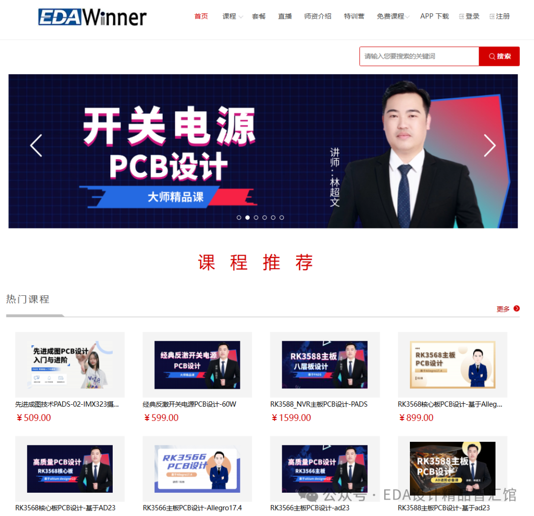
◉ Video Tutorials: PCB Engineer Fast-Track Training Camp, Student Class Video Tutorials
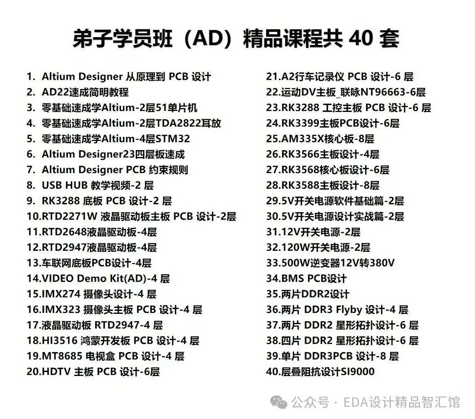
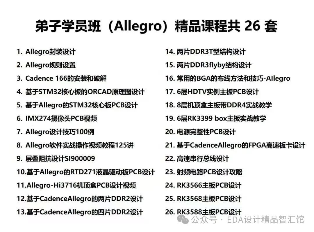
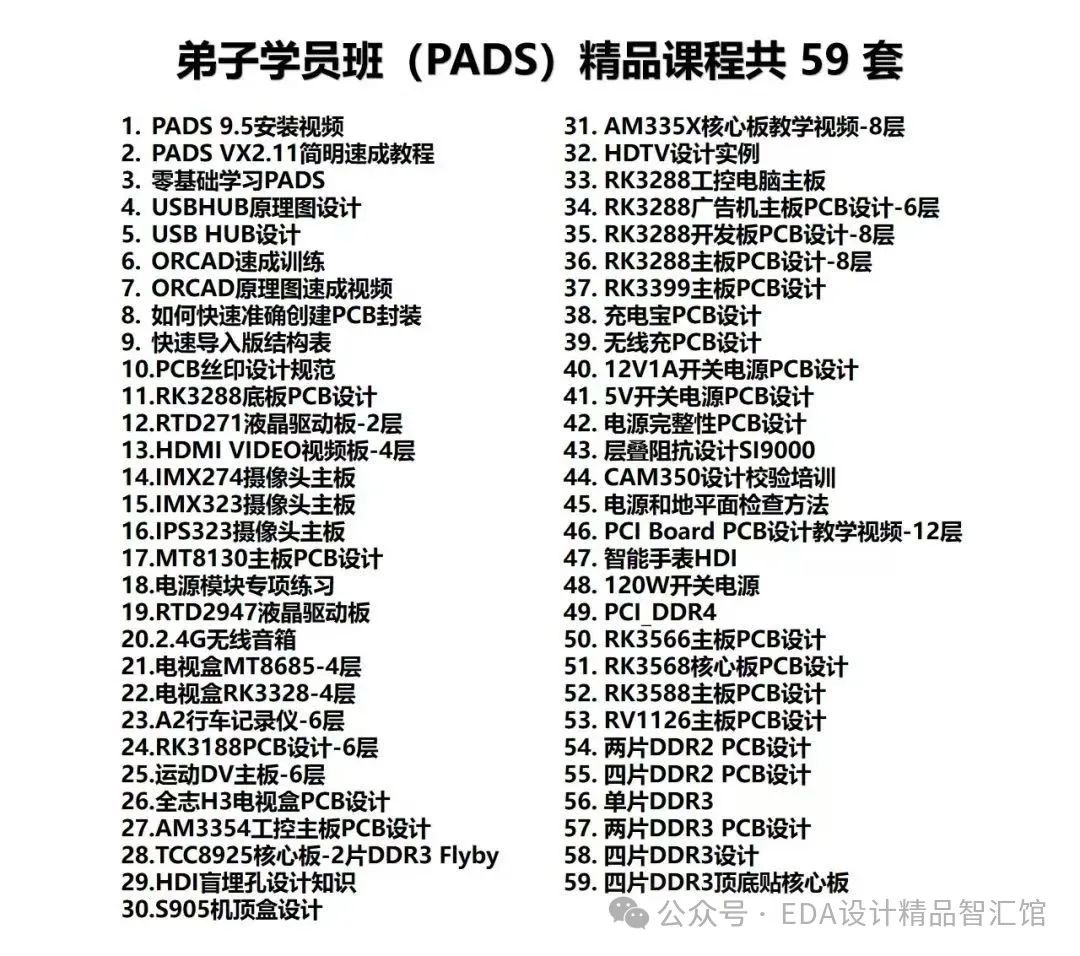
◉ Training: “Full-time High-Speed PCB Training Camp”, “Sunday High-Speed PCB Training Camp”
2025 High-Speed PCB Design Training
EDA Wuyou Academy
High-Speed PCB Training Camp

?
Why Learn High-Speed PCB Design?
With the rapid development of the electronics industry, the demand for PCB design engineers continues to grow, and salary levels remain at the forefront of technical positions. Having specialized PCB design skills can help you stand out in the job market and increase your chances of obtaining high-paying positions.
Regarding Career Development
☑ Broad employment prospects
☑ High salary benefits
☑ Expanded career development paths
☑ Meeting the technical update needs of the industry
Regarding Skill Enhancement
☑ Learning systematic knowledge
☑ Practical operational experience
☑ Improving design quality and reliability

01
Course Introduction
PCB design is based on circuit schematics to realize the functions required by circuit designers. Excellent PCB design can save production costs and achieve good circuit performance and heat dissipation. An excellent PCB designer is a comprehensive knowledge entity, requiring solid hardware circuit knowledge, understanding of electronic component characteristics, as well as knowledge of SI, PI, EMC, thermal design, and process design.
This course mainly introduces high-speed and high-density PCB design technologies and related engineering cases, through systematic teaching, continuously summarizing the hardware design and layout design rules for each product, accurately analyzing the functional principles and key points of PCB design for mainstream products, and systematically detailing the entire PCB design of products, enabling students to quickly master and produce excellent PCB designs through modular circuit design and systematic learning.
Class Start Time:Enroll Anytime
Training Format:Full-time offline instruction
Learning Period:Full-time 2/4 months
Training Software:Altium, PADS, Allegro
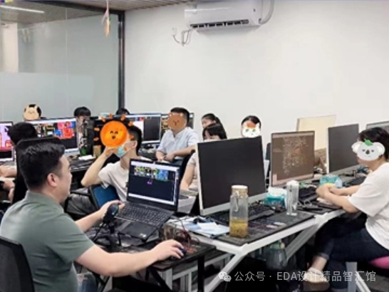
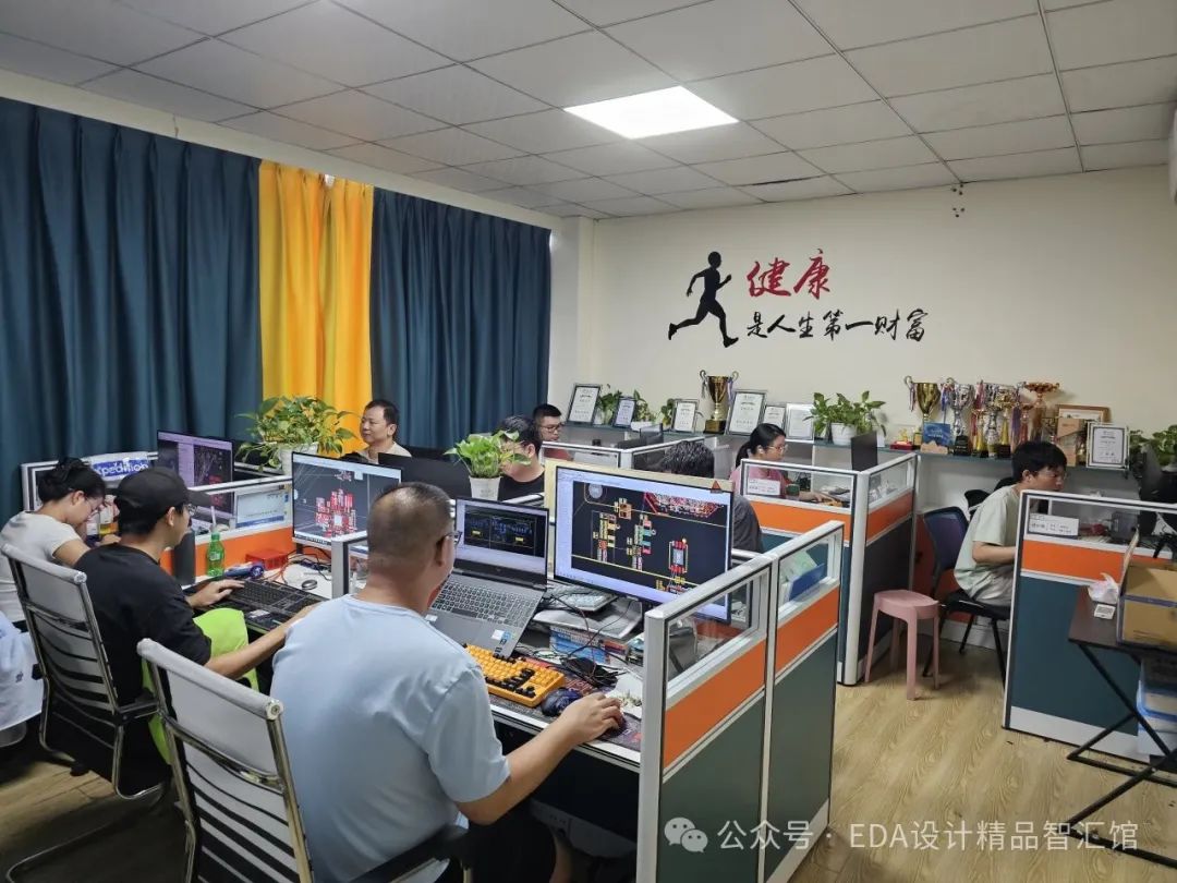
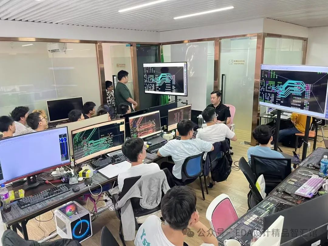
Learning Method:Offline instruction + case explanation + practice guidance (Every Monday to Friday (9:00~18:00) for 2~4 hours of class, with the remaining time for students’ practical work, where teachers guide students and provide technical support.)
After-Sales Service: Sign a training contract, provide employment and interview guidance, and offer lifelong free technical support.
Training Location:Fuhai Cultural and Creative Park E403, E412, Bao’an District, Shenzhen
Shenzhen Indawino Circuit Technology Co., Ltd.
Scan to Get Group Purchase Price | Enrollment Consultation👇



Enroll for Learning | 15013440483 (WeChat same number)

About Us
EDA Wuyou Academy continues to focus on cultivating talents in EMC, simulation, hardware, high-speed PCB design, and other fields. Firmly adhering to the teaching philosophy of “practical teaching, experiential teaching, real-time teaching”, and committed to continuously supplying high-skilled comprehensive talents to society through leading technology, high-quality teaching cases, and practical teaching models. We have established good cooperative relationships with many enterprises, forming a good reputation in the industry. Through internet education, technical salons, training classes, and collaborations with electronic publishers to publish multiple EDA textbooks, we have helped hundreds of thousands of engineering technicians and university faculty and students improve their technical capabilities.

High-Level PCB Engineer Certificate
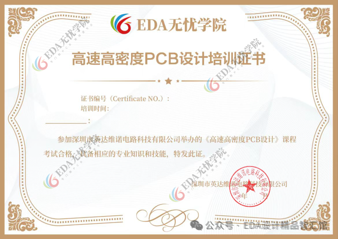
EDA Wuyou Academy Training Certificate
02
Instructor Team

Lin Chaowen
Chief Instructor of EDA Wuyou Academy
Chief instructor at EDA Wuyou Academy, with over 20 years of management experience in hardware interconnect design, proficient in various PCB design and simulation tools such as Cadence, Mentor, PADS, AD, HyperLynx. Author of multiple EDA books, with a series of books referred to by industry professionals as the “High-Speed PCB Design Bible”.

Zhou Peng
Gold Instructor of EDA Wuyou Academy
Gold instructor at EDA Wuyou Academy, with rich PCB design experience, proficient in various mainstream PCB design software such as Cadence, PADS, AD, etc.

Nana
Gold Instructor of EDA Wuyou Academy
Gold instructor at EDA Wuyou Academy, with rich practical PCB design experience, helping students master practical skills through real case teaching.
03
Target Audience
◉ Struggling to improve skills without formal channels
◉ Looking to increase salary
◉ Simply interested in this technology
◉ Students or graduates aiming to enhance market competitiveness
◉ Engineers of other EDA software
◉ Looking to transition to PCB engineers
04
Training Arrangement
Introduction to PCB Design Software
PADS/AD/Allegro
Master the basic operations and design techniques of the software.
Modular Design
Common Module Design
PCB layout and wiring design specifications for power modules, USB/HDMI interface modules, BGA, storage modules, etc., understanding design points and precautions for different modules.
Practical Cases
2-8 Layer Project Full Process Practice
Analyze the layout ideas and optimization processes of different types of electronic products (such as consumer electronics, industrial control boards, switch power supplies, etc.) through practical cases.
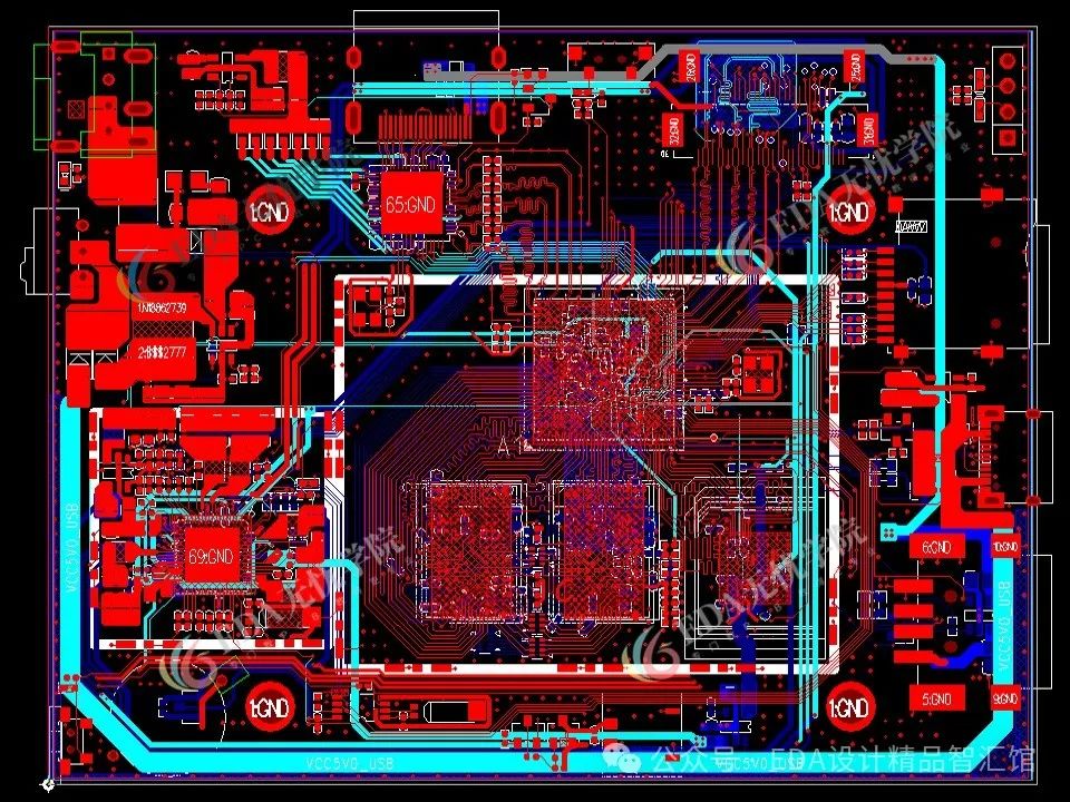
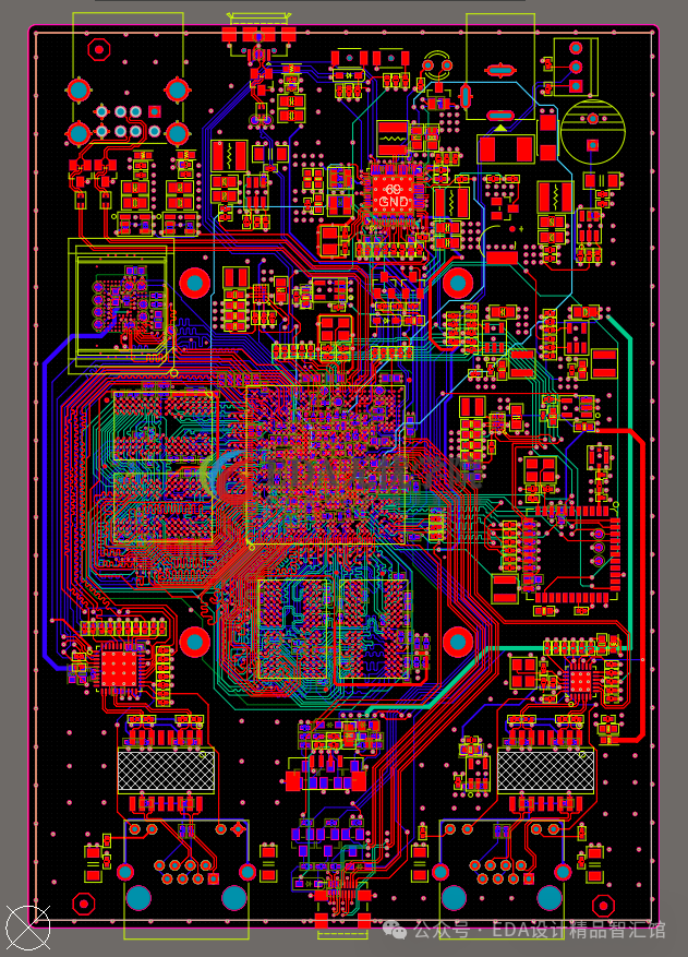
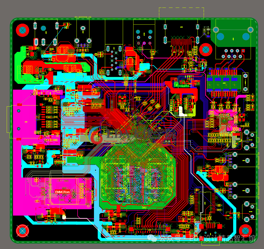
Practical Training
Simulating Corporate Project Operation Models
Simulating the actual project operation models of enterprises, cultivating students’ teamwork and communication coordination skills, while deepening understanding and mastery of theoretical knowledge and design processes in practice, understanding industry needs and standards, enhancing employment competitiveness.
Employment Guidance
Corporate Recommendations
Resume writing and optimization, interview guidance, excellent student employment recommendations
Enrollment
Strategy
01
Enrollment enjoys group purchase discounts
02
Enrollment grants access to student class video courses
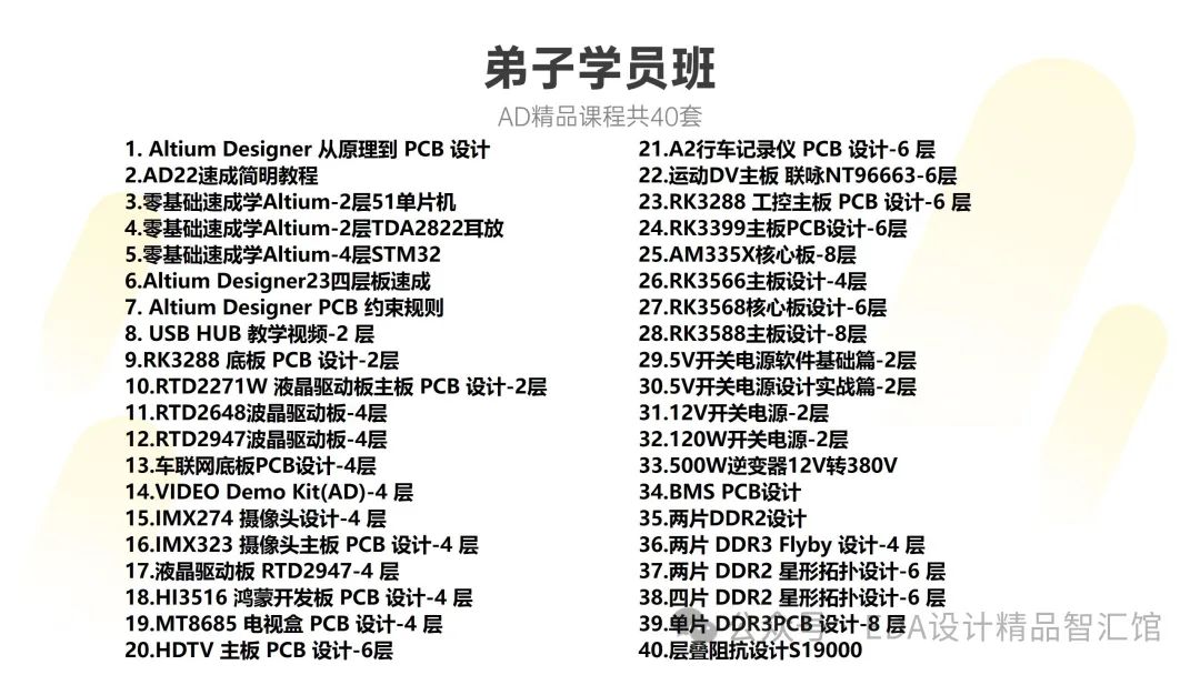
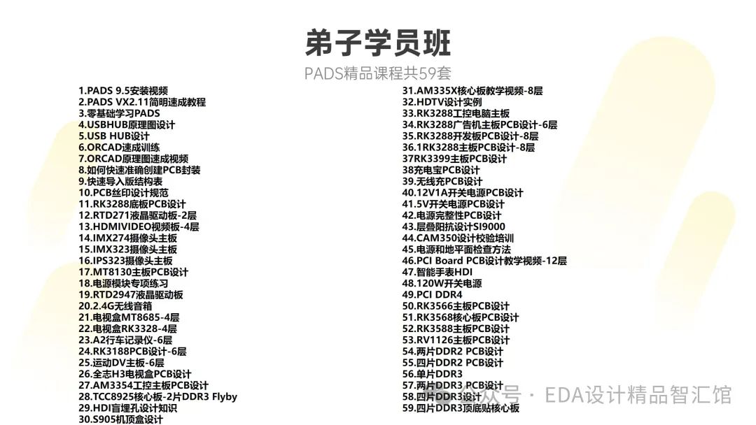
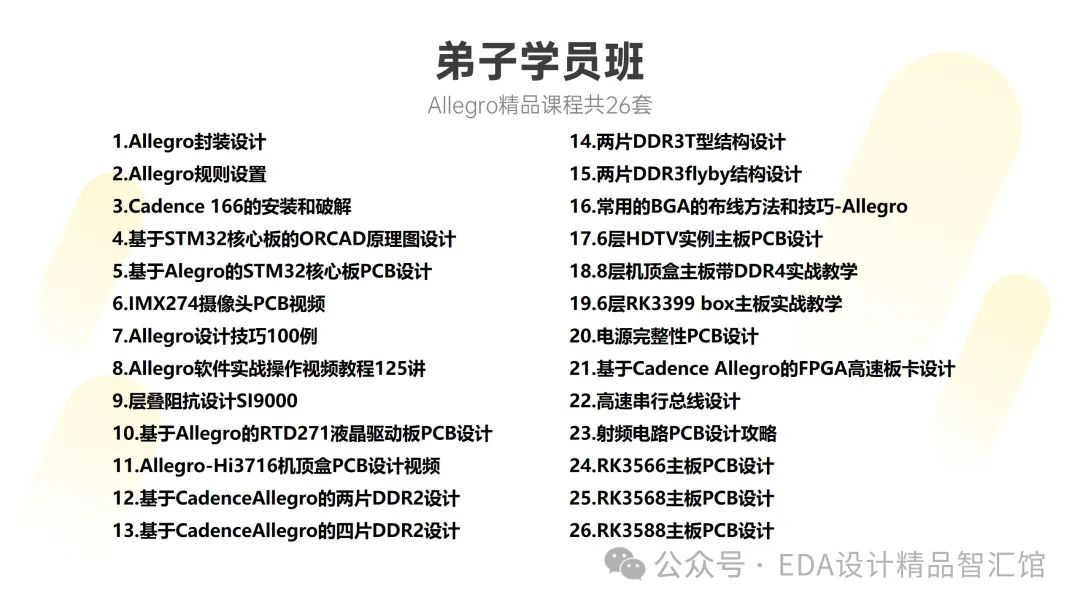
Swipe left to unlock more photos
03
If you cannot attend the full-time course, you can also enroll in our Sunday class
Training Format:Sunday online or offline
Class Start Time:March 2
Learning Period:4 months
Training Software:Altium + PADS, Allegro
Learning Method:Face-to-face or live broadcast + case explanation + homework review, Online and offline synchronous teaching (providing class playback videos)
Training Location:
Offline: Fuhai Cultural and Creative Park E403, E411, E412, Bao’an District, Shenzhen
Online: Tencent Meeting
✦✦

Scan to Consult
Get more course information
WeChat Enrollment| 15013440483