Source: Content from http://www.cnblogs.com/IClearner/, Author: IC_learner, thank you.
Previously, we learned about the purpose of low power design and the composition of power consumption. Today, I will share some insights on power analysis. Since this learning is aimed at front-end design of digital ICs, the power analysis here is based on the power compiler tool in DC; for more precise power analysis, PT can be used. For power analysis using PT, please refer to other materials, as we will not cover PT usage for power analysis here.
(1) Overview of Power Analysis and Process
In the previous section, we explained the composition of power consumption and briefly introduced the calculation of power consumption in conjunction with the technology library. However, in reality, we cannot manually calculate the power consumption of actual large-scale integrated circuits. We often rely on EDA tools to help us analyze the power consumption of circuits. Here, we will introduce the (general) process of analyzing power consumption using EDA tools, and in the next section, we will introduce the design and optimization of low-power circuits.
① Input and Output of Power Analysis Process
The process of power analysis (from the perspective of input-output relationships) is shown below:
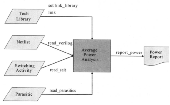
In the diagram above, four items are needed:
-
tech library: This contains the power consumption information of the technology library, and a more precise library should also contain state path (SDPD) information provided by the foundry.
-
netlist: The gate-level netlist circuit of the design, which can be obtained through DC synthesis.
-
parasitic: Parasitic parameters such as parasitic capacitance and parasitic resistance in the design, which are generally provided by backend RC parasitic parameter tools. Simple power analysis may not require this file.
-
switch activity: Contains the switching behavior of each node in the design, such as the flip rate of nodes or files that can calculate the flip rate of nodes. This switching behavior input file is very important. This switching behavior can be provided in different forms, leading to different methods of analyzing power consumption later.
(Note that regardless of the method used for power analysis, the input design file is always the gate-level netlist file.)
② Some Concepts of Switching Behavior
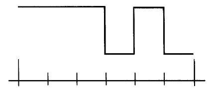
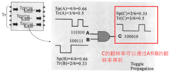
When it comes to switching behavior, the flip rate we discussed earlier is also a type of switching behavior. Additionally, we have other concepts related to the description of switching behavior. Here, we will illustrate this with examples, as shown in the figure below:
-
Number of flips: The number of logical changes. In the above figure, the number of flips of the signal is 3.
-
Flip rate: As previously mentioned, the flip rate is the number of flips of the signal (including clock, data, etc.) per unit time. In the above figure, the flip rate is 3/6 = 0.5 (3 flips in 6 time intervals).
-
T1, T0: The duration of the logic values of the (node) signal being 1 and 0. In the above figure, T1 is 4, and T0 is 2.
-
Static probability (SP): The probability of the (node) signal logic value being 1. In the above figure, SP is 4/6 = 2/3.
③ Representation of Switching Behavior (File) Situation
Earlier, we mentioned that power analysis requires the situation of switching behavior, generally referring to the flip rate of each node. We have the following ways to set the flip rate:
Direct command: For example, the command:
set_switching_activity -static 0.2 -toggle_rate 20 -period 1000 [all_inputs]
In this case, the node with the flip rate set is the input, and the corresponding flip rate is: Tr = 20/1000 = 0.02GHz
-
SAIF file: The switching activity interchange format file used for exchanging information between simulators and power analysis, which is an ASCII file (American Standard Information Interchange code file).
-
VCD file: The value change dump file, which is also an ASCII file, includes the change information of the selected variable values in a design. This information is obtained by using the “VCD system function” in the simulation testbench.
In Synopsys’s low-power design process, power analysis can be performed using the power compiler (included in the design compiler). We can analyze power consumption by defining the flip rate of nodes through commands—this is called the vector-free analysis method; since SAIF and VCD files can be obtained through circuit simulation, they are simulation interface format files. Therefore, when more precise results are needed, SAIF or VCD files are generally used (VCD files can be converted to SAIF files using related commands, and then SAIF is used for power analysis).
(2) Vector-Free Analysis Method
Earlier, we mentioned that the vector-free analysis method is to analyze power consumption by defining the flip rate of nodes through commands. First, we will learn what commands are needed, and then we will provide examples of vector-free analysis scripts.
Before learning to set the flip rate commands, let’s first understand what the propagation starting point and black box of the design are. We define the propagation starting point as the input end of the design and the output end of the black box. A black box refers to a unit (such as ROM, RAM, or some IP core) that does not have a functional description in the technology library.
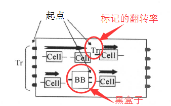
In the above design, there are three starting points: one is the input end of the entire design, one is the output end of the black box, and the last one is the input end of a certain unit. The last starting point is not included in our definition, but we also treat it as a starting point because it is marked with a flip rate, which we will explain later.
When analyzing power consumption using the vector-free analysis method, we do not need to provide the flip rate of internal nodes of the design but only need to set the flip rate of the starting points. We have two methods to set the flip rate: one is through setting flip variables, and the other is through marking methods. Below we will introduce how to set the flip rate using these two methods.
① Setting Flip Variables
In the power compiler, we can set the following two flip variables to set the flip rate:
power_default_toggle_rate
power_default_static_probability
Next, we will introduce these two variables (mainly focusing on power_default_toggle_rate).
power_default_toggle_rate: Its usage can be found by running man in DC. This variable sets the default flip rate used in the design. The definition method is:
set power_default_toggle_rate flip_value
The default flip value is 0.5. This flip value is not the flip rate; the flip rate defined by this variable is a relative value:
-
If the design defines a clock, the variable power_default_toggle_rate defines the flip rate based on the fastest clock. For example, if the flip value is 0.5 and the fastest clock in the design is 10ns, then the flip rate Tr = 0.5/10ns = 0.05GHz, which means the default flip rate for the entire design is 0.05GHz.
-
If there is no clock in the design, it will reference the time unit in the technology library. For example, if the time unit in the technology library is ns and the flip value is 0.5, then the flip rate Tr = 0.5/1ns = 0.5GHz.
power_default_static_probability: This sets the default static probability, which is the probability that the logic value at the starting point is 1. As for static probability, we will not describe it in detail here. The default flip values for both variables are 0.5, and the flip rate is generally quite large, so it is usually necessary to reduce it a bit, such as setting it to 0.01 or 0.02.
Generally, the default flip rate is set at the starting point, meaning that the flip rate at the starting point uses the flip rate set by the variable power_default_toggle_rate, and the flip rate of internal nodes can be obtained through propagation, as shown in the figure below:
It should be noted that propagation cannot pass through black boxes that do not have functional descriptions, meaning that the output flip rate of a black box cannot be obtained through propagation. Therefore, we defined the output of the black box as a starting point earlier, so that the flip rates of other nodes can be obtained through propagation (including the input of the black box). The output flip rate of the black box is obtained through the default flip rate setting, allowing us to obtain the flip rates of all nodes in the design.
② Marking Flip Rate
The method described above sets the default flip rate. When we need to mark a specific flip rate for a certain node rather than using the default flip rate, we use the marking flip rate, as shown in the figure below:
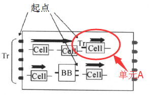
The input port of unit A is marked with a specific flip rate, for example, 0.04GHz. The marked flip rate takes precedence over the propagated flip rate, and the node with the marked flip rate will be treated as a new starting point. This does not belong to the definition of starting points, but we still refer to it as a starting point because the flip rate is marked. After marking the flip rate, the flip rates of subsequent nodes will be propagated from this newly marked flip rate.
The commands to set the marked flip rate (referred to as setting flip rate) mainly include two:
set_switching_activity and set_case_analysis. Below, we will explain the meanings of these two commands.
set_switching_activity: Sets the flip rate and static probability of a certain node. This command is widely used when estimating power consumption using the vector-free analysis method. The command and options are as follows:
set_switching_activity
[-static_probability static_probability]
[-toggle_rate toggle_rate]
[-state_condition state_condition]
[-path_sources path_sources]
[-rise_ratio rise_ratio]
[-period period_value | -base_clock clock]
[-type object_type_list]
[-hierarchy]
[object_list]
[-verbose]
Below we will briefly introduce a few commonly used options; detailed introductions can be obtained by running man set_switching_activity.
-static_probability: Sets the static probability.
-period period_value | -base_clock clock: Sets the clock (period); either -period or -base_clock can be set.
-toggle_rate: Sets the flip value, associated with -period or -base_clock. The flip rate Tr equals: the number of flips in the time period specified by the -base_clock option or the number of flips in the time period specified by the -period option. If neither of these options is set, the time unit in the technology library will be used, meaning the flip rate equals the number of flips in each library unit time.
Now let’s provide examples to illustrate the usage of this command:
Example 1:
create_clock CLK -period 20
set_switching_activity -base_clock CLK -toggle 0.5 -static 0.015 [all_inputs]
The above command sets the clock period to 20ns, and then the command uses the -base_clock option. The flip value for all inputs is 0.5, and the static probability is 0.015, resulting in a flip rate Tr = 0.5/20 = 0.025 GHz.
Example 2:
set_switching_activity -period 1000 -toggle 25 -static 0.015 [all_inputs]
The above command does not create a clock but uses the period option, indicating that there were 25 flips in 1000 periods, thus we can obtain the flip rate for all inputs Tr = 25/1000 = 0.025 GHz.
Example 3:
set_switching_activity -toggle 0.025 -static 0.015 [all_inputs]
In the above command, neither the -period nor the -base_clock options are used. At this time, it is related to the time unit in the technology library. If the time unit in the library is ns, then we get the flip rate Tr = 0.025 /1 = 0.025 GHz.
The above explains the set_switching_activity command. Next, we will explain the set_case_analysis command.
set_case_analysis is used to specify a static logic value, which means setting the signal to a constant without flipping. Some signals in the design need to be designed this way, such as reset signals, set as follows:
set_case_analysis 1 [get_ports reset]
Then, the value of reset is set to always be 1.
We have discussed how to set the flip rate. Below, we will provide examples to illustrate how to use these two flip rates in combination. For the design below:
The requirements for setting the flip rate are as follows:
1. Correctly define the clock;
2. Use the set_case_analysis command to set the constant control signal reset;
3. Set the flip rate at the transmission starting point, setting any known flip rate at the input end and the output end of the black box. The other starting points will use the default flip rate.
4. Allow the tool to propagate the flip rate in the design.
The above does not require specific flip rates, so we can set the flip rates we want. Based on the above requirements, we write the corresponding TCL script as follows:
create_clock -p 4 [get_ports clk]
set_case_analysis 0 reset [get_ports reset]
set_power_default_toggle_rate 0.003
set_switching_activity -tog 0.02 a
set_switching_activity -tog 0.06 b
set_switching_activity -tog 0.11 x
In the above script, the clock period is set to 4(ns), and then the set_case_analysis command is used to set the reset port as a constant. The flip value is 0.003, so the corresponding flip rate is 0.003/4ns, which is the default flip rate. Then, the set_switching_activity command specifies the flip values for a, b, and x, with their flip rates being flip value/4ns.
We previously introduced the vector-free analysis method for power analysis. Before introducing the method of using SAIF files for power analysis, we will first explain the concepts of synthesis invariant objects and synthesis variant objects, as shown in the following diagram of an RTL design and gate-level design:
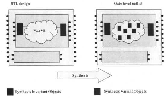
According to the definition, the number and structure of registers in the design remain unchanged before and after synthesis, the input/output ports and hierarchical boundaries remain unchanged, and the black boxes in the design remain unchanged. These unchanged objects are called synthesis invariant objects. Most combinational circuits generated in the design are closely related to design constraints, and different constraints produce different combinational circuits. These changing objects are called synthesis variant objects. Since the SAIF file involves these two concepts, we introduce them here.
After introducing these two concepts, let’s learn about using SAIF files for power analysis. There are two ways to use SAIF files as flip rate input files, meaning there are two methods for power analysis using SAIF: RTL backward SAIF obtained from simulating RTL code and gate backward SAIF obtained from simulating gate-level netlists. Below we will introduce each in detail.
(3) SAIF–RTL BACK Analysis Method
RTL backward SAIF files are obtained by simulating RTL code. When the design is large, the time required for gate-level simulation is long, so this method can be used for analysis. The speed of power analysis using this method is relatively fast, but it is not as precise as the SAIF file from gate-level simulation.
① RTL Forward SAIF File
RTL forward SAIF files are files that record the switching behavior of synthesis invariant objects in RTL designs. It can be simply understood that RTL forward SAIF files briefly record the flip rates of synthesis invariant objects. The generation of RTL backward SAIF files requires RTL forward SAIF files, so we first need to produce RTL forward SAIF files. The process of generating RTL forward SAIF files is as follows:
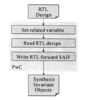
RTL forward SAIF files are generated by the power compiler (included in the design compiler). According to the process, we know that we mainly set some variables, then read in the RTL design (RTL.v design), and finally read out the SAIF file. The corresponding script is as follows:
set power_preserve_rtl-hier_names true
read_verilog “sub.v top. v”
rtl2saif -output fwd_ rtl.saif
An example of part of an RTL forward SAIF file is as follows:
(SAIFILE
(SAIFVERSION “2 .0”)
(DIRECTION “forward”)
(DESIGN)
(DATE “Wed May 12 18:31:19 2004”)
(VENDOR “Synopsys,Inc”)
(PROGRAM NAME “rtl2saif”)
(VERSION “1 .0”)
(DIVIDER/)
(INSTANCE top
(PORT
(address\15\ address\15\)
(address\14\ address\14\)
(address\13\ address\13\)
(address\12\ address\12\)
(address\11\ address\11\)
(address\10\ address\10\)
······
We can see that the file contains a series of synthesis invariant objects in the design. During subsequent simulations, the simulator only monitors the switching behavior of these objects.
② Generation of RTL Backward SAIF Files
Below is the process of generating RTL backward SAIF files:
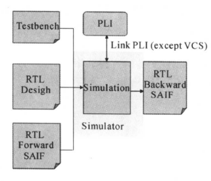
From the above diagram, we know that generating RTL backward SAIF files requires inputting the testbench file, RTL.v design, and RTL forward SAIF file in the simulator. We will introduce each of these components below.
· First, the PLI. To generate SAIF files using VCS, the Programming Language Interface (PLI) is needed to monitor node flips and obtain the flip rates of nodes. The main system tasks needed are:
$set_gate_level_monitoring ( on|off|rtl_on);
$set_toggle_region (obj);
$read_ rtl_ saif(rtl_saif_file_name,tb_pathname);
$toggle_start;
$toggle_stop;
$toggle_reset();
$toggle_report(file_name,type,unit);
· RTL.v is the design source file, and the RTL forward SAIF file has been discussed earlier, so we will skip that here.
· Finally, the testbench. The testbench calls the RTL design, the above-mentioned PLI system functions, and the RTL forward SAIF file, etc. A simple example of a testbench file is as follows:
module testbench;
top instl (a, b, c,s);// Instantiate the top design
initial begin
$read_rtl_saif (“myrtl.saif”)
$set_toggle_region (u1);
$toggle_start;
#120 a=0;
#STEP in_a=temp_in_a;
······
$toggle_stop;
$toggle_report(“rtl.saif”,1.0e-9,”top”);
end
endmodule
In the above testbench, the system task program $read_rtl_saif (“myrtl. saif”) reads in the synthesis invariant object file—RTL forward SAIF. Therefore, during simulation, the simulator only monitors the switching behavior of these synthesis invariant objects. The command $set_toggle_region (u1) selects the module to monitor. The commands $toggle_start and $toggle_stop control the start and end times of monitoring. The command $toggle_report(“rtl. saif”,1. 0e-9,”top”) outputs SAIF information to the specified file.
With everything ready, we can now run the simulation using VCS:
vcs -R rtl. v testbench. v
Note that here we are simulating the RTL design file. After the simulation is completed, we can obtain the rtl.saif file, which is the RTL backward SAIF file.
③ Power Analysis
After simulating the RTL code, the obtained RTL Backward SAIF file contains the switching behavior information of synthesis invariant objects in the design. During power analysis, the analysis tool propagates the flip rates of synthesis invariant objects through its internal simulator, thus obtaining the flip rates of all other nodes for gate-level circuit power analysis. Once we have the RTL backward SAIF file, we can analyze power consumption according to the previous process of power analysis (from the perspective of input-output relationships):
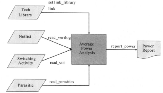
Here, the switching activity file is the RTL backward SAIF file. Then, the process of using the power compiler to analyze power consumption with the RTL backward SAIF file is as follows:
An example script for this process is as follows:
set target_library my. db
set link_library “* $target_library”
read_verilog mynetlist.v
current_design top
link
read_ saif -input rtl.saif -inst testbench/top
report_power
The process of analyzing power consumption using the RTL backward SAIF file is as described above. The above process and script are applicable for pre-layout designs and do not use parasitic parameter files. The RC parameters of the wiring use the load model from the technology library. If it is a post-layout design, parasitic parameter files should be used to improve the accuracy of power analysis.
From the above, we know that the process of analyzing power consumption using RTL backward SAIF files is as follows:
power compiler generates RTL forward SAIF file ——》VCS simulation generates RTL backward SAIF file ——》power compiler analyzes power consumption.
(4) SAIF–GATE Analysis Method
Previously, we introduced the method and process of analyzing power consumption using RTL backward SAIF files. Next, we will introduce the method and process of analyzing power consumption using gate backward SAIF files, which is very similar to that of RTL backward SAIF files.
① Library Forward SAIF File (referred to as Library SAIF File)
Library SAIF files are SAIF files that contain SDPD (State Path) information. The generation of gate backward SAIF files requires library SAIF files, which can be generated by the power compiler. The process is as follows:
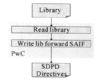
An example script for this process is as follows:
read_db mylib.db
lib2saif -output mylib. saif -lib_pathname mylib.db
Part of an example library SAIF file is as follows:
(SAIFILE
(SAIFVERSION “2.0” “lib”)
(DIRECTION “forward”)
(DESIGN)
(DATE “Mon May 10 15:40:19 2004”)
(VENDOR “Synopsys,Inc”)
(PROGRAM NAME “lib2saif”)
(VERSION “1 .0”)
(DIVIDER / )
(LIBRARY “ssc_core_typ”
(MODULE “and2al”
(PORT
(Y
(COND A RISE FALL (IOPATH B)
COND B RISE FALL(IOPATH A)
COND DEFAULT)
)
······
Library SAIF files contain SDPD information. With library SAIF files, during simulation, the simulator will monitor the switching behavior of nodes based on the SDPD information in the library.
② Generation of Gate Backward SAIF Files
Below is the process of generating gate backward SAIF files:
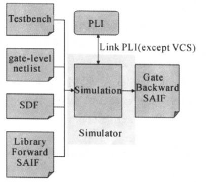
From the above diagram, we can see that generating gate backward SAIF requires the testbench, gate-level netlist, standard delay format (SDF) file, and library SAIF file. The SDF file reflects the RC delay parameters in the gate-level netlist, which can provide a more accurate delay for the wiring.
The example content of the testbench is as follows:
module testbench;
top instl (a, b, c,s);
initial
$sdf_annotate(“my.sdf”,dut)
initial begin
$read_lib_saif (“mylib.saif”);
$set_toggle_region (u1);
$toggle_start;
#120 a=0;
#STEP in_a=temp_in_a;
······
$toggle_stop;
$toggle-report(“gate.saif”,1.0e-9,”top”)
end
endmodule//testbench
The testbench mainly calls the gate-level netlist, SDF file, and library SAIF file. In the testbench, the command $sdf_annotate(“my. sdf”, dut) marks the SDF to ensure timing correctness, thus obtaining the correct flip count. The command $read_lib_saif (“mylib. saif”) reads the SDPD information from the library SAIF file. The simulator only monitors the switching behavior listed in the SAIF file. The command $set_toggle_region (u1) selects the module to monitor. The commands $toggle_start and $toggle_stop control the start and end times of monitoring. The command $toggle_report(“gate. saif”,1. 0e-9, “top”) outputs SAIF to the specified file.
Everything is ready, and the next step is to run the simulation using VCS:
vcs -R top.v testbench. v
Note that here we are simulating the gate-level netlist, meaning that the top.v is the gate-level netlist. Part of the generated example gate forward SAIF file is as follows:
(SAIFILE
(SAIFVERSION “2.0”)
(DIRECTION “backward”)
(DESIGN)
(DATE “Mon May 17 02:33:48 2006”)
(VENDOR “Synopsys,Inc”)
(PROGRAM_NAME “VCS-Scirocco-MX Power Compiler”)
(VERSION “1 .0”)
(DIVIDER / )
(TIMESCALE 1 ns)
(DURATION 10000.00)
(INSTANCE tb
(INSTANCE top
(NET
(z\3\
(T0 6488) (T1 3493) (TX 18)
(TC 26) (IG 0)
)
······
(z\32\
(T0 6488) (T1 3493) (TX 18)
(TC 26)(IG 0)
)
······
)
(INSTANCE U3
(PORT
(Y
(TO 4989) (T1 5005) (TX 6)
(COND((D1 * !DO)|(! D1*D0)) (RISE)
(IOPATH S (TC 22 )(IG 0)
)
COND((D1*!DO)}(!D1,DO))
( IOPATH S (TC 21)(IG 0) (FALL)
)
COND DEFAULT (TC 0)(IG 0)
)
······
Gate Backward SAIF files are obtained by simulating the gate-level netlist. If the design is large, the time required for simulation is long. The advantage is that the accuracy is very high. The Gate Backward SAIF files generated by VCS contain some or all of the switching behaviors of wires and units. These switching behaviors are represented by rising and falling edges and are related to state and path. This information can be used for precise power analysis.
③ Power Analysis
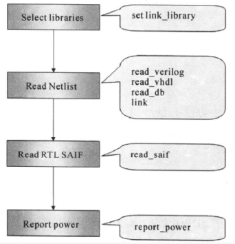
With the gate-level netlist, gate backward SAIF file, and SDF file, power analysis can be performed in the power compiler. The process of analyzing power consumption is as follows:
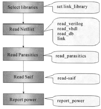
An example script file for this process is as follows:
set target_library mylib.db
set link_library ” * $target_library”
read_verilog mynetlist.v
current_design top
link
read_read_parasitics top.spef
read_ saif -input mygate. saif -inst tb/top
report_power
The above process and script are applicable for post-layout designs, where the spef file is generated after layout completion. Using parasitic parameter files improves the accuracy of power analysis. If it is a pre-layout design, the wiring’s RC parameters use the load model from the technology library.
Finally, to summarize, the process of analyzing power consumption is as follows:
power compiler generates library SAIF files——》VCS generates gate backward SAIF files——》power compiler analyzes power consumption.
(5) VCD to SAIF Analysis Method
We have introduced the methods of analyzing power consumption using SAIF files, which are obtained through VCS simulation. Next, we will introduce the method of converting VCD files to SAIF files and then analyzing power consumption.
① Generation of VCD Files
First, when we perform simulations, we need to include relevant system functions in the testbench to generate the corresponding VCD file (and SDF file). The process is illustrated as follows:
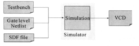
An example testbench is as follows:
module testbench;
······
initial
$sdf_annotate(“my.sdf”,dut)
initial begin
$dumpfile(“vcd.dump”);
$dumpvars;
······
end
Then use the following command to run the simulation:
vcs -R dut.v testbench.v +delay_mode_path
After completing the simulation, we can obtain the VCD file.
② Converting VCD Files to SAIF Files
The VCD files generated during simulation also contain the switching behavior of nodes and wires in the design. In the Power Compiler, the program vcd2saif can be used to convert VCD files into SAIF files, as shown in the figure below:
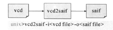
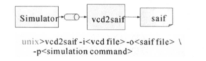
vcd2saif is a program used in the UNIX command line. The vcd2saif program can also convert VPD files (binary format VCD files) into SAIF format files. If the design is large and the simulation time is long, the vcd2saif program can use a pipeline to convert VCD to SAIF files. In this case, the VCD file is not stored in a file; instead, the VCD data is passed to the vcd2saif program through FIFO (First-In First-Out), generating the SAIF file. The converted SAIF file does not contain SDPD information. As shown in the figure below:
Once we have the SAIF file, we can analyze power consumption using SAIF files as previously described, whether for pre-layout or post-layout power analysis, depending on whether there is layout-related information, such as an SPEF file. Therefore, the process is:
VCS generates VCD files——》power compiler converts VCD files to SAIF files——》power compiler analyzes power consumption.
Finally, let’s discuss the benefits of using the vcd2saif program, mainly three points:
1. VCD generation is fast;
2. VCD is an IEEE standard and suitable for post-simulation;
3. The conversion process is fast.
We have introduced four methods to generate switching behavior for designs: directly setting flip rates, RTL backward SAIF files, gate backward SAIF files, and VCD to SAIF files; these methods can be mixed, and their priority order is as follows:
The switching behavior marked by the read_saif command has the highest priority; the switching behavior set by the set_switching_activity command has the second priority; and the lowest priority is the flip rate specified by the default variable power_default_toggle_rate.
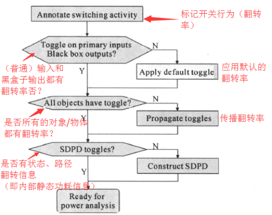
Switching behavior can be cleared; the command “reset_switching_activity” can clear all marked flip rates and flip rates obtained through propagation. The command report_saif can display the switching behavior information in the design after reading the SAIF file. A complete SAIF file should have a “user annotated” of 100%. If the SAIF is incomplete, the default flip rates will be added to the input ends and the output ends of black boxes. The flip rates will be propagated through zero-delay simulation, allowing the power consumption of the design to be calculated.
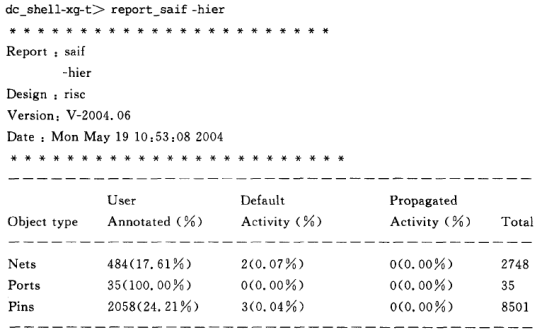
An example of using the report_saif command is as follows:
The commands related to switching behavior include:
merge_saif # Merge SAIF files
read_sai f # Read backward SAIF files
report_saif # Report switching behavior information
rtl2saif # Generate RTL forward SAIF files
write_ saif # Write a backward SAIF file
lib2saif # Generate library forward SAIF files
propagate_switching_activity # Propagate power consumption clearing
reset_switching_activity # Clear switching behavior and/or flip rates
set_switching_activity # Set switching behavior on specified objects
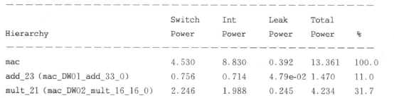
(6) Power Analysis Report
We check the design power consumption through the power analysis report (generated by the report_power command), and a sample part of a power report is as follows:
Cell Internal Power=883.0439 mW(66%)
Net Switching Power=453.0173 mW(34%)
Total Dynamic Power=1 .3361 W(100%)
Cell Leakage Power = 391.5133 nW
Where the first item is the internal short-circuit power, the second item is the switching power, and together they constitute the dynamic power; the last item is the static power, also known as leakage power. If you want to report the power consumption of each module and unit in the design, you can add the option -hier after the report_power command, for example: report_power -hier, and the generated report is as follows: