With the popularity of IoT devices, the security issues of these devices have gradually been uncovered by “interested parties”. For example, in September 2017, a hacker analyzed the firmware of ofo shared bikes, discovering four attack methods and controlling the shared bike [1]; in October 2017, the LIFX smart bulb was successfully hacked because the firmware leaked key-related information [2]; at the ReCon BRX 2018 conference, two researchers from Northeastern University reverse-engineered the internal firmware of Xiaomi IoT devices and found vulnerabilities in the entire Xiaomi ecosystem [3].
Why do researchers and hackers want to obtain the firmware of IoT devices when studying them, and how do they obtain this firmware? The vulnerabilities mentioned in these three cases were discovered because the firmware of the IoT devices was obtained by researchers and then reverse-engineered. More cases can be found on the official websites of ReCon and BlackHat conferences. By analyzing the chain of attacks on IoT devices, I found that they obtain the firmware, reverse it into assembly or C programming language, which allows them to analyze the device’s operating process and network behavior, and also find information related to security encryption keys. If these “interested parties” cannot obtain the firmware information, they would find it difficult to discover these vulnerabilities. From this perspective, the security of IoT devices largely depends on the security of their firmware.
Are there ways to prevent “interested parties” from obtaining the firmware? To answer this question, it is essential to understand how firmware is stored in IoT devices and clarify the methods for obtaining IoT device firmware. Next, I will present the security of IoT device firmware focusing on the storage methods, acquisition methods, and protective measures.
From the perspective of computer architecture (using the von Neumann architecture as an example), firmware is stored in memory to facilitate CPU addressing, reading instructions, and interpreting instructions. “Interested parties” can determine the storage location of firmware in IoT devices by knowing which components in the device have the capability to store firmware.
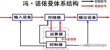
Figure 1. Von Neumann Architecture
Knowing that the firmware is in memory is not enough; it is also necessary to know which part of the memory the firmware is located in. Because data in memory is read and written based on addresses, “interested parties” must know the address where the firmware is written by the manufacturer to fully obtain the firmware’s location information.
If the firmware is stored in memory, it can certainly be found on the mainboard of the IoT device, thus locating the firmware of the IoT device. Generally, the way firmware is stored on the mainboard can be roughly divided into two categories: integrated and separated, as shown in Figures 2 and 3.
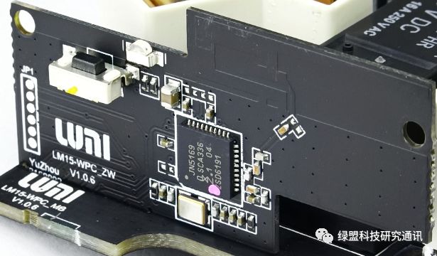
Figure 2. Integrated Storage
Figure 3. Separated Storage
Integrated Firmware Storage
When the device’s functions are relatively simple and do not require a complex operating system or an integrated complex protocol stack, and do not require sufficient computing power, manufacturers generally integrate the firmware into their main control chips to save costs. We will temporarily refer to these devices as weak devices.
The composition of weak devices is quite different from that of personal computers. Generally speaking, personal computers have very large hard drives (over 10GB) to store operating systems to meet the normal operation of the operating system; whereas almost all weak devices only require firmware with a capacity of hundreds of kilobytes to operate normally. To meet the needs of system integration, main controller manufacturers (such as ST, NXP, etc.) integrate the memory (RAM), hard drive (Flash and other rewritable non-volatile memory), CPU (computing core), and peripheral interfaces (for communication with peripheral devices) into a single chip. This chip, which is usually used for simple control of sensors, motors, and other peripheral devices, is also known as a microcontroller unit (MCU), which is what we commonly refer to as the main controller. As shown in Figure 4.
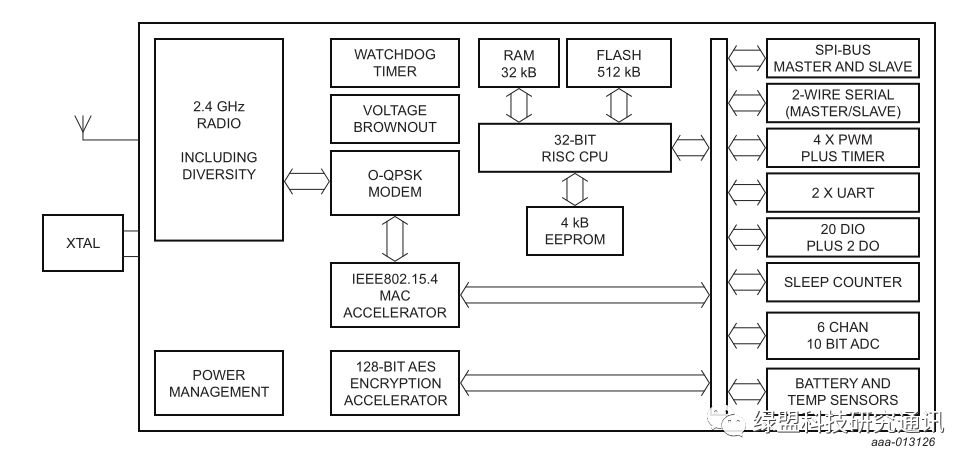
Figure 4. Composition of JN5169 Main Control Chip (with RF Function)
From the perspective of the internally integrated 32bit RISC CPU, its addressing capability can reach 2^32 bytes, which is 4GB. The internal firmware is certainly stored in ROM, which is FLASH or EEPROM. Generally, the device’s firmware is written to FLASH, while EEPROM is used for important system parameters or data storage.

Figure 5. Memory Address Function Distribution of JN5169
As shown in Figure 5, within the addressable 4GB space, the FLASH area address space is 0x00080000~0x00100000 (512KB). As long as “interested parties” can obtain data from this address space through some method, the firmware is obtained. The method will be introduced in the next chapter; next, I will introduce the separated case.
Separated Firmware Storage
When the internal storage capacity of the main controller cannot completely store the required firmware or information, manufacturers generally connect external storage to the main controller. Generally, there are three types of storage, as shown in Figure 6 (the three chips below). Correspondingly, the above devices can be used as modules to read the storage below, which can be inserted into a computer to read the firmware using the supporting software. At this time, “interested parties” do not need to know how the address mapping of these three types of storage is in the main controller or CPU; they can directly remove the chip and read it using the corresponding module.
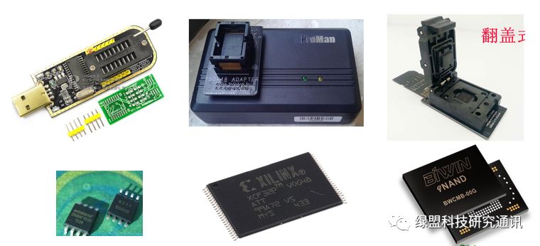
Figure 6. Three Types of External Storage
But if these chips are not removed, is there a way to read them? Yes, through bootloader or using debugging interfaces like JTAG/SWD, the firmware content can be read by controlling the read and write process of the main controller. Reading firmware content using this method requires knowing where this storage is mapped in the main controller to the firmware in memory, similar to the firmware address of JN5169, which will not be elaborated here.
1Network Upgrade Interception (FTP, HTTP)
Firmware can be obtained not only locally. When IoT devices enter the upgrade process, the specific path for upgrading firmware through the network can be obtained by capturing the traffic information during the upgrade process, thus reproducing the firmware upgrade process to acquire the firmware.
For example, in the upgrade process of a certain camera, the IoT device requests the FTP server and then downloads the firmware, as shown in Figure 7.
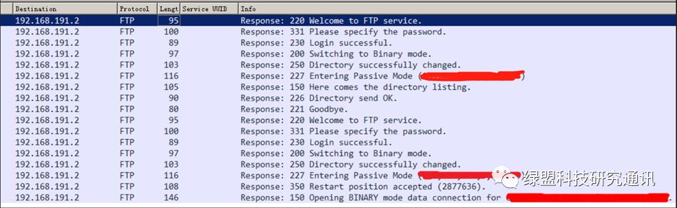
Figure 7. FTP Upgrade Process of a Certain Camera
Similarly, in the upgrade process of a certain IoT device, the IoT device initiates a GET request to the cloud via the HTTP protocol and subsequently acquires the firmware, as shown in Figure 8.
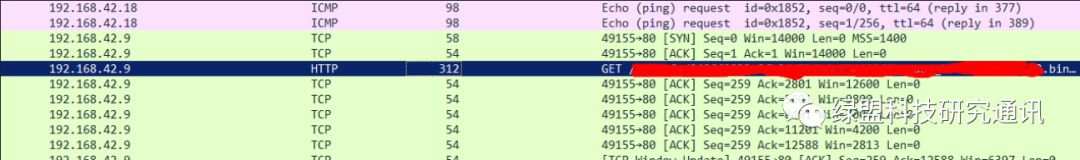
Figure 8. A Certain IoT Device’s HTTP Upgrade Process
The method of capturing network upgrade traffic to obtain firmware is suitable for capturing packets immediately after purchasing the device, as some devices upgrade firmware silently, which users are unaware of. If the device adopts a silent upgrade method and the device happens to have the latest firmware version, it will not enter the upgrade process, and the firmware cannot be obtained through the upgrade. At this point, “interested parties” will use other methods introduced in this chapter to acquire the firmware.
2Directly Reading Storage Chips
In the previous chapter, we introduced the location of firmware in the mainboard under the separated firmware storage method. This section describes how “interested parties” directly read data from storage to obtain firmware.
Since the storage is directly removed by welding, soldering tools are necessary, as shown in Figure 9. After the attacker removes the storage, they will use a programmer, as shown in Figure 11, to read the firmware from the storage, as shown in Figure 10. The reading methods for the other two types of storage are similar to this process and will not be elaborated here.

Figure 9. Desoldering Station
Figure 10. Storage of a Certain Router
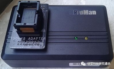
Figure 11. NAND Flash Chip Programmer
In addition to this programmer, “interested parties” will also obtain supporting software from the seller, which runs on a PC to read the contents of the NAND flash, as shown in Figure 12. By using this software and programmer, after establishing a connection between the storage chip and the PC, they can directly read the firmware.
Figure 12. Upper Computer Used for Reading NAND Flash
3Reading via Serial Port or Other Communication Buses
The methods mentioned in the previous section are quite brute-force. Among the ways “interested parties” can acquire firmware, there is also a relatively “gentle” method, which is to establish communication through the exposed UART interface on the mainboard between the PC and the bootloader program embedded in the main controller, thus reading the firmware by controlling the process of reading instructions from the firmware. Using the STM32 microcontroller as an example, this section describes how to utilize the internal bootloader of the main controller to obtain the code in the flash area.
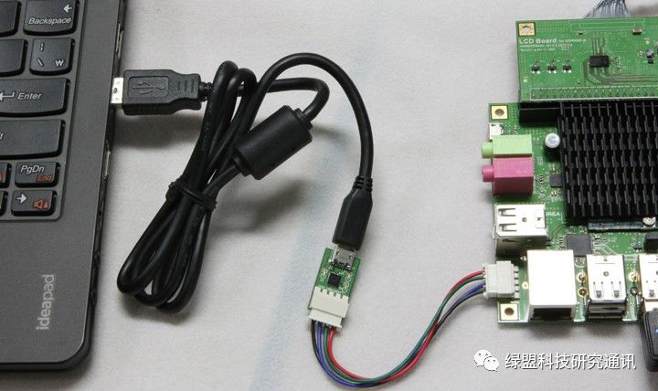
Figure 13. PC Communicating with Target Device via UART Bus
Regarding the bootloader, ST provides the following description for its STM32 series products:
“The bootloader is stored in the internal boot ROM memory (system memory) of the STM32 device. It is programmed by ST during production. Its main task is to download the application program to the internal Flash via a usable serial peripheral (USART, CAN, USB, I2C, etc.). Each serial interface defines a corresponding communication protocol, which includes a compatible command set and sequence.” [5]
From the official introduction, the main role of this bootloader is to facilitate chip users (embedded software developers) to download firmware programs to the flash area of the main controller. In fact, besides this function, the bootloader also has the capability to read firmware. This will be discussed in the entire operation process of the bootloader.
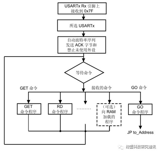
Figure 14. Bootloader Startup Process
From the startup process [6], if the bootloader is activated (usually set by the state of hardware pins), the main control chip will remain in a command-waiting state, allowing another host (such as a PC connected to the main controller via a serial bus) to send commands through serial communication to download firmware to memory or read content from memory. If the host sends an RD command, it will enter the process of reading internal data from memory.
When the slave receives 0x11+0xEE from the host, the host will then transmit the address of the data to be read and the size of the data to the slave, which will then send the data back to the host. At this point, as long as the host stores the received data as a binary or hexadecimal file, the firmware can be obtained. The data reading process is shown in Figure 15.
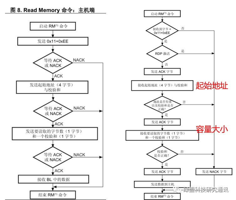
Figure 15. Bootloader RD Command Process – Host Side (Left)/Main Controller (Right)
Using the bootloader to read other MCUs is similar; refer to the official documentation for the description of its bootloader program. If the official chip manual does not provide a communication process and timing for reading firmware via external communication interfaces, it indicates two possibilities: first, the company producing the chip does not intend to open the method to read firmware via bootloader; second, the company has not designed the circuit for reading firmware via external communication interfaces into the chip. In either case, the manufacturer has closed or prohibited the method to obtain firmware via bootloader. For example, Renesas Electronics (MCU manufacturer) does this.
4Reading via Debugging Interfaces
Some products expose interfaces used for hardware development and debugging on the mainboard, such as JTAG/SWD interfaces. Generally, if only using serial ports, it is not possible to set breakpoints during the development and debugging phase, so manufacturers implement JTAG/SWD hardware modules to facilitate developers to dynamically debug the code running on the chip via a hardware debugger as a communication protocol adapter. Using the SWD interface as an example, this section describes how to establish a connection between the PC and the IoT device using the wiring method shown in Figure 16.
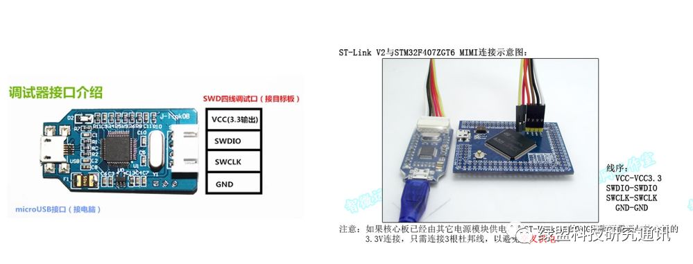
Figure 16. SWD Wiring Method
Once the connection between the PC and the main control chip is established, it is necessary to refer to the communication protocol specifications of the SWD interface to read the data stored in flash to obtain the firmware. Unlike reading firmware via bootloader, manufacturers of hardware debuggers provide supporting software as host programs, such as J-Link driver programs, etc., allowing the PC to write data to the main controller’s memory, read data, execute instructions, set breakpoints, etc., achieving hardware debugging effects.
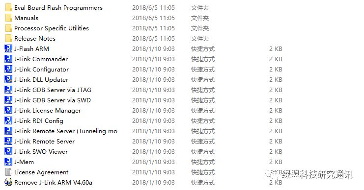
Figure 17. Supporting Software for J-Link Driver
Taking the J-Link driver program as an example, the J-Link driver program is paired with the J-Link hardware debugger. After installing the J-Link driver program on the PC, software like that shown in Figure 17 will be included. Running J-Link Commander and J-Flash ARM can establish a connection between the PC and the chip and read the firmware. J-Link GDB Server via SWD/JTAG can establish a GDB debugging service, allowing for dynamic debugging of the main control chip using the usual gdb.
Firmware can be adequately protected. The previous two chapters discussed the location of firmware and reading methods. From these introductions, if the device exposes UART or JTAG/SWD interfaces, the firmware may be read. If the firmware is stored separately, it may not be possible to prevent the firmware from being read through software programming. If we want to adequately protect the firmware, the most basic requirement is to prevent “interested parties” from easily reading it.
1Encrypted Transmission and Authentication
To prevent firmware from being obtained by “interested parties” in a local area network, it is necessary to incorporate encrypted transmission and request authentication into the product’s upgrade process.
If the product requests FTP service, it can replace it with SFTP service and perform mutual authentication. This way, the content they see is encrypted file transfer traffic, and without the information needed for decryption, they cannot decrypt the data packets. Additionally, authentication related to keys can prevent man-in-the-middle attacks. SFTP service is implemented based on SSH service, so the mutual authentication process can be set by configuring the SSH service; specific methods can be found in relevant documents or tutorials online, which will not be elaborated here.
If the product requests HTTP service, it can replace it with HTTPS service and perform mutual authentication. There are many setups for HTTPS encrypted communication and mutual authentication based on nginx and apache available online, which will not be presented here.
However, how should the device achieve transmission encryption and authentication? I will take the Kaa [7] (version 0.10.0) open-source IoT solution as an example to illustrate how the IoT device side should be designed to achieve secure authentication and transmission encryption.
From the Kaa architecture diagram, Kaa generates an SDK for IoT devices, and engineers using Kaa can download the SDK source code from the server for compilation and operation, thus connecting to the Kaa server. I analyzed the source code of the Kaa SDK and came to the following conclusions:
1. Data transmission between Kaa server and device side is based on AES256 encryption.
2. The Kaa server authenticates the device side, but I did not find authentication for the cloud side.
3. The device side uses the AES key as a signed text and adopts the RSA signing method.
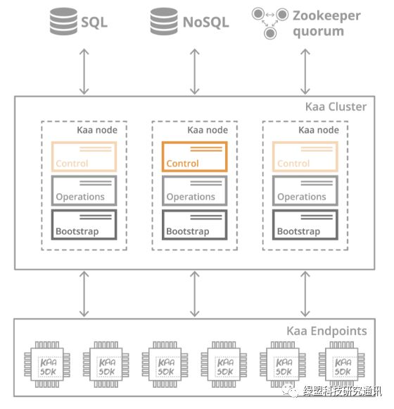
Figure 18. Overall Architecture of Kaa
The encryption method of Kaa is strong enough. Currently, its signature authentication uses unidirectional authentication. How can we change Kaa’s unidirectional authentication to mutual authentication? On the device side, after establishing a TCP connection, before transmitting the signed information of the device, a process for authenticating the server should be added. The authentication method can also use another RSA secret key, enabling the device to have the server’s signature verification key when generating the SDK, thus authenticating the server. On the server side, an independent authentication service can be opened, dedicated to encrypting transmission authentication information.
However, it is essential to note that we need to protect the private key adequately, placing the key in an area of the chip that can perform read protection to prevent attackers from obtaining cloud key information. The method for setting read protection will be illustrated with a case in section 4.3 of this chapter.
2Hiding Interfaces
How to hide UART, JTAG, and other debugging interfaces? I provide the following ideas:
1. Hide the main control chip’s pins and model information.
Using BGA packaged chips can effectively hide the chip’s pins, increasing the difficulty of determining the debugging interface’s location. If the chip’s model information is also erased, “interested parties” will not have specific documents to refer to, making it challenging to determine the chip model and thus the interface location. If the mainboard retains pads for these two types of interfaces, they can only blindly test through these pads to determine the interface location.
Figure 19. BGA Packaged Chip
2. Remove the pads and related silkscreen for these two types of interfaces on the mainboard.
If the wiring and pads related to these two types of interfaces are deleted from the mainboard, “interested parties” can only contact the BGA packaged chip’s pins by removing the main control chip. If they want to read the firmware, they must establish a connection with the PC by pulling out wires. If the firmware is stored separately, removing the chip will not allow reading the firmware from the external storage via the main control chip, as even if the PC establishes a connection with the chip, the connection between the storage and the chip has been disconnected. At this point, they can only read the firmware from the internal flash of the main control chip or directly remove the storage chip and read the firmware from it.
Deleting pads, silkscreens, and chip information, and hiding chip pins, these two methods have limited “interested parties” to only two methods for reading firmware: removing the storage or main control chip and using other tools to obtain firmware through brute force.
3Setting Read Protection for Main Control Chips
Setting read protection within the main control chip can prevent “interested parties” from reading the firmware in the internal flash area. Taking the RDP read protection feature provided by STM32 main controllers as an example, if the read protection operation is set for the internal storage area, it is necessary to remove the read protection before reading the internal storage area, and the operation to remove read protection will erase the storage area. In fact, if the read protection mechanism is removed, the firmware in the main control chip has already been erased. Therefore, this method can prevent “interested parties” from violently removing the main controller and reading the internal flash data separately to obtain the firmware.
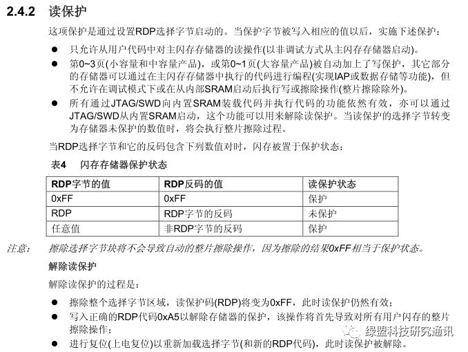
Figure 20. Official Description of STM32 RDP Read Protection
To date, products with integrated storage firmware can adequately protect their firmware, making it nearly impossible for “interested parties” to read the firmware in the main controller. The methods available to “interested parties” are now limited to products with separated storage, where they can remove the storage chip and then read it using a programmer.
4Encryption Protection
If specific protective circuits are not added, it is impossible to prevent “interested parties” from reading the firmware from external storage. As a fallback, we can encrypt part of the firmware to prevent them from obtaining useful information (such as the file system) from it. For example, encrypting all code except the bootloader, with the decryption program implemented in the bootloader. The information related to the decryption key can be placed in the main controller and protected by read protection, so even if they obtain the encrypted firmware and the algorithm in the bootloader, they cannot obtain the decryption key and access useful information.
In summary, if we can comprehensively utilize encryption technology, read protection technology, and pay attention to hiding interfaces and chip information during product development, it is challenging for “interested parties” to read the device firmware or obtain useful information from it. Without firmware and without interfaces to access the system console, they can only blindly test the device, thereby ensuring the security of the IoT device to a certain extent.
All content in this article is limited by my limited knowledge and may inevitably have omissions. If you believe that the content presented in this article is incorrect or have different opinions on the views expressed in this article, I welcome you to point it out and communicate with me at any time.
References:
[1]. ofo bike hacking case, http://news.ifeng.com/a/20170906/51893522_0.shtml
[2]. How to hack LIFX smart bulb, https://weibo.com/ttarticle/p/show?id=2309404160876054708433
[3]. Reversing IoT: Xiaomi ecosystem – Dennis Giese, Daniel Wegemer, https://recon.cx/2018/brussels/resources/slides/RECON-BRX-2018-Reversing-IoT-Xiaomi-ecosystem.pdf
[4]. JN5169 Chip Manual, https://www.nxp.com/docs/en/data-sheet/JN5169.pdf
[5]. STM32™ Microcontroller System Memory Boot Mode, https://www.st.com/content/ccc/resource/technical/document/application_note/b9/9b/16/3a/12/1e/40/0c/CD00167594.pdf/files/CD00167594.pdf/jcr:content/translations/zh.CD00167594.pdf
[6]. USART protocol used in the STM32 bootloader, https://www.st.com/content/ccc/resource/technical/document/application_note/51/5f/03/1e/bd/9b/45/be/CD00264342.pdf/files/CD00264342.pdf/jcr:content/translations/en.CD00264342.pdf
[7]. Kaa SDK Reference Document, https://kaaproject.github.io/kaa/docs/v0.10.0/Getting-started/
[8]. Von Neumann Architecture, https://www.zhihu.com/question/28774776
[9]. Green米 ZigBee Smart Wall Socket Disassembly, http://www.geekifix.com/thread-534-1-1.html
[10]. Xiaomi Router Disassembly, https://post.smzdm.com/p/567861/
[11]. Desoldering Station, https://detail.tmall.com/item.htm?spm=a230r.1.14.6.7bca5668RKO7yd&id=8845676872&cm_id=140105335569ed55e27b&abbucket=10
[12]. USB to Serial Connection Method, https://wiki.odroid.com/accessory/development/usb_uart_kit
[13]. J-LINK OB Connection Method, https://item.taobao.com/item.htm?id=550202959975&ali_refid=a3_430582_1006:1110675646:N:j-link+ob:2cd1448a20aa458e10c06e7dd8ba2392&ali_trackid=1_2cd1448a20aa458e10c06e7dd8ba2392&spm=a230r.1.14.6#detail
Content Editor: IoT Security Laboratory Zhang Kelei Editor: Xiao Qing
Previous Issues Review
-
Hackers are exploiting Drupal vulnerabilities for client browser mining
-
Introduction to Network Protocol Reverse Engineering – Netzob Overview and Pros and Cons Analysis
-
Threat Intelligence Practical Implementation – From Grey to Black
-
[Recruitment] Green Alliance Technology Innovation Center Internship Recruitment Announcement (Long-term Valid)
This public account’s original articles only represent the author’s views and do not represent the position of Green Alliance Technology. All original content copyright belongs to Green Alliance Technology Research Communications. Unauthorized reproduction, reprinting, excerpting, or other use by any media or WeChat public account is strictly prohibited. Reprinting must indicate the source as Green Alliance Technology Research Communications and include a link to this article.
About Us
Green Alliance Technology Research Communications is operated by the Green Alliance Technology Innovation Center, which is the cutting-edge technology research department of Green Alliance Technology. It includes the Cloud Security Laboratory, Security Big Data Analysis Laboratory, and IoT Security Laboratory. Team members consist of PhDs and Masters from key universities such as Tsinghua, Peking University, Harbin Institute of Technology, Chinese Academy of Sciences, and Beijing University of Posts and Telecommunications.
As one of the important training units of the “Zhongguancun Science and Technology Park Haidian District Postdoctoral Workstation Branch,” the Green Alliance Technology Innovation Center conducts joint training with Tsinghua University for postdoctoral researchers. Research results have covered various national project topics, national patents, national standards, high-level academic papers, and published professional books.
We continuously explore cutting-edge academic directions in the field of information security, starting from practice, combining company resources and advanced technologies to achieve concept-level prototype systems, and then delivering product line incubation products to create significant economic value.

Long press the QR code above to follow us