Introduction: In the previous article, we introduced the manufacturing process of PCBs, but we would like to delve deeper into the aspects of via copper thickness and the aspect ratio of PCB vias.
Definition of PCB Copper Thickness
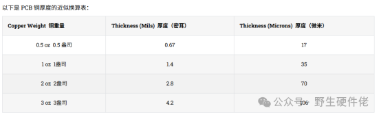
The thickness of copper in a circuit is measured in ounces (oz). So, why is thickness expressed in weight units?
Definition of an ounce (oz):
When 1 ounce (28.35 grams) of copper is flattened to cover an area of 1 square foot (0.093 square meters), its thickness is 1.4 mil.
The weight of copper is measured in ounces per square foot (oz/ft2).
The table below shows the relationship between the weight of copper and its thickness (in mils and micrometers).
First, let’s discuss how vias in PCBs are plated, which requires a reference to the previous article;
Refer to the previous article: “Step-by-Step Guide to PCB Manufacturing Process“
After the drilling stage, PCBs typically undergo a plating process, where a layer of conductive material, such as copper, is coated inside the holes. This is to provide electrical connections between different layers of the PCB. This plating method can be either chemical deposition or electroplating, with electroplating being used to thicken the copper.
This process is commonly referred to as first copper (this plating is not just for vias but for the entire board, hence it is also called board plating).
During the outer layer etching process, electroplating is used to coat the retained traces with a layer of copper, during which excess copper on the outer layer is removed. This process is commonly referred to as second copper (since it is electroplating for the surface image, it is also called image plating).
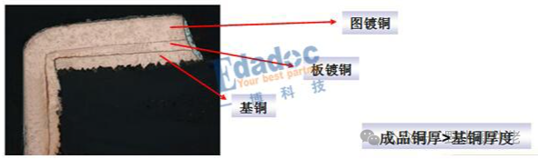
From the above two images, we can clearly see that the final copper thickness of the PCB is the sum of the base copper thickness of the PCB plus the final thickness of board plating and image plating. In other words, the completed copper thickness is greater than the base copper of the PCB, while the total via copper thickness is completed through both processes, namely the thickness of the copper plated in the vias and the thickness of the copper plated for the patterns.
The conventional finished copper thickness of 1 OZ, with via copper according to IPC Class 2 standards, typically has a thickness of 5-7um for first copper (board plating) and 13-15um for second copper (image plating), resulting in via copper thickness between 18-22um. Considering etching and other losses, the final via copper thickness is around 20um.
According to IPC-6012 standards:
Class 1 and Class 2 require an average copper plating thickness of at least 20 micrometers, with thin areas not less than 18 micrometers;
Class 3 requires an average copper plating thickness of at least 25 micrometers, with thin areas not less than 20 micrometers.
The same requirements apply to blind vias, but not to microvias that do not have a via barrel and have lower plating requirements.
Aspect Ratio of PCB Vias

As shown in the figure above, the aspect ratio (thickness-to-diameter ratio, translated here as aspect ratio) refers to the diameter D of the hole divided by the thickness H of the PCB (equal to the length of the barrel).
The aspect ratio is an important metric for both PCB designers and manufacturers, as it reflects the reliability, cost, and manufacturability of the circuit board. Firstly, the aspect ratio can indicate the manufacturability of vias (and any plated through holes on the circuit board) and reveal potential issues with the plating strength of the via barrel.
To explain this, a brief introduction to the electroplating process of vias is needed:
a. The electroplating process for PCB vias begins after the PCB has been thermally pressed.
b. The internal layers of the PCB have been etched, but the copper on the top and bottom layers has not yet been etched.
c. At this stage, through holes are drilled, which are not plated and are not conductive.
d. All holes undergo multiple cleaning processes to remove debris generated during the drilling stage.
e. A small amount of conductive carbon is placed inside the holes to be plated, acting as a metal seed layer to allow subsequent copper to grow on it.
f. The copper layers on the top and bottom are connected to a voltage source, and the entire panel is immersed in an electrolyte bath containing copper ions.
g. The entire panel acts as a conductor, allowing current to flow from the plating solution to the panel. Any exposed metal areas (including through holes) will be plated by absorbing copper ions from the plating solution.
h. The vias are now plated, and the next step is to etch the copper on the top and bottom layers. A protective tin coating is applied to the pads at the top and bottom of the vias (including the walls of the holes) to protect them from the next etching step.
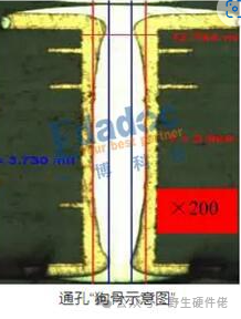
Now it can be understood why vias with a high depth-to-diameter ratio are easier to plate. The larger the hole diameter, the easier it is for the chemical solution containing copper ions to flow into the hole. Similarly, the longer the barrel (i.e., the thicker the PCB), the more difficult it is to plate the interior of the barrel. Regardless of the aspect ratio, the center of the barrel (approximately located in the middle between the top and bottom) is always the hardest area to plate because fewer copper ions reach that area—thus, this area is more prone to failure.
When the aspect ratio is high, the walls of the vias exhibit a “dog bone” phenomenon.
Empirically, when the hole diameter exceeds 10 mil, the aspect ratio can be set at 1:10; however, for hole diameters of 8 mil or smaller, a smaller aspect ratio is required, which means the PCB thickness must also be thinner. The following summarizes the allowable aspect ratios:
1. 12 mil (300um) finished hole – Aspect ratio 1:10 – Maximum board thickness 3mm
2. 10 mil (250um) finished hole – Aspect ratio 1:10 – Maximum board thickness 2.5mm
3. 8 mil (200um) finished hole – Aspect ratio 1:8 – Maximum board thickness 1.6mm
4. 6 mil (150um) finished hole – Aspect ratio 1:6.6 – Maximum board thickness 1mm (only for advanced processes)
Reference list:
1. https://zhuanlan.zhihu.com/p/26553259
2. https://www.elepcb.com/blog/pcb-copper-thickness/
3. https://www.protoexpress.com/kb/copper-for-pcbs/
4. https://www.epiccolo.com/articles/pcb-vias-guide