 With the rapid development of artificial intelligence technology, the global demand for efficient, low-power, high-performance computing chips is becoming increasingly urgent. ASIC (Application-Specific Integrated Circuit) is a type of chip customized for specific tasks, and its outstanding performance, power efficiency, and cost-effectiveness are making it a key force in driving the implementation of AI technology. From cloud service giants to tech startups, from data centers to edge devices, the application scenarios for ASICs are continuously expanding, and the market size is steadily growing. This article will deeply analyze the market prospects, architecture and ecosystem, industry chain, and competitive landscape of related companies in the ASIC industry, exploring the application prospects and development opportunities of ASICs in the AI era, providing comprehensive and in-depth insights for industry practitioners and investors.
01
Industry Overview
1. Concept of ASIC Chips
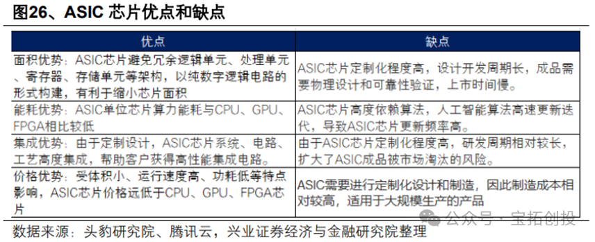
AI chips mainly include GPUs, FPGAs, and ASICs. AI ASICs are custom integrated circuits designed specifically for artificial intelligence applications, characterized by high performance, low power consumption, customization, and low cost. The main reason is that ASICs eliminate redundant designs, making them suitable for executing specific tasks with excellent energy consumption performance; at the same time, ASICs exhibit low computation latency and high peak computational capability in task adaptation, performing exceptionally well in areas such as AI edge inference and deep learning training, far surpassing CPUs in executing similar tasks. Due to these advantages, companies like Google and Cambricon are actively investing in ASIC research. Of course, ASICs also have their limitations. For example, they have a high degree of customization, long development cycles, and poor flexibility, making them difficult to reuse when algorithms are upgraded or tasks change. 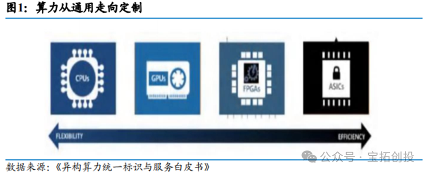
2. Classification of ASIC Chips
ASICs can be further subdivided into TPUs, NPUs, DPUs, and other ASIC chips. TPUs are AI processors invented by Google, primarily supporting tensor computations. DPUs are used for accelerated computing within data centers, while NPUs correspond to the CNN convolutional algorithms from the previous AI boom, which have since been integrated into many SoCs for edge device processing chips.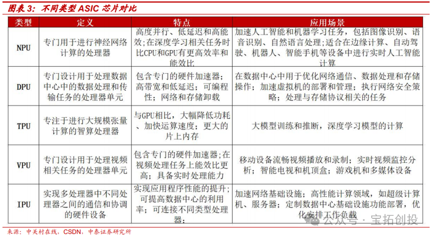 ASIC chips are also divided into fully customized ASIC chips, semi-custom ASIC chips, and programmable ASIC chips. (1) Fully Customized ASIC Chips: Fully customized ASIC chips are among the highest in terms of customization, where developers design logic units for different functions based on various circuit structures, building analog circuits, storage units, and mechanical structures on the chip board. Fully customized ASIC chips perform excellently in terms of performance and power consumption. The average computational output of fully customized ASIC chips is about 8 times that of semi-custom ASIC chips, and fully customized ASIC chips manufactured using a 24nm process outperform semi-custom ASIC chips made with a 5nm process. (2) Semi-Custom ASIC Chips: The logic units that make up semi-custom ASIC chips are mostly derived from standard logic unit libraries, with some custom designs based on specific requirements. 1) Gate array chips: Gate array ASIC chips include channel gate arrays, non-channel gate arrays, and structured gate arrays. The structure of gate array ASIC chips has predetermined transistor positions on the silicon wafer that cannot be changed, and designers often adjust the interconnection structure of logic units by changing the metal layers at the bottom of the chip; 2) Standard cells: This type of ASIC chip is composed of logic units selected from standard cell libraries. Designers can arrange standard cells according to algorithm requirements. (3) Programmable ASIC Chips: PLDs, also known as programmable logic devices, include a matrix of basic logic units, flip-flops, latches, etc., with their interconnection parts existing as a single module. Designers program PLDs to meet certain custom application requirements.
02
Market Prospects
1. Cloud Providers’ Self-Developed ASICs as Key Increment for AI Chips
Currently, NVIDIA still occupies a major supplier position in the AI accelerator card market, but the proportion of self-developed ASICs by cloud providers is gradually increasing. The competitive landscape of AI accelerator cards mainly includes three types of “players”: 1) Global leader NVIDIA; 2) Other commercial AI accelerator companies, such as AMD, Intel, and Ascend; 3) Cloud providers’ self-developed ASICs. According to Trendforce statistics, in 2022, NVIDIA held a 67.6% market share in the global AI chip market, and its market share is expected to decline by 2024, while the proportion of AMD and other cloud providers’ self-developed ASICs is expected to increase. Cloud providers’ self-developed ASICs will become the most core source of incremental AI chips in the future. On one hand, self-developed accelerator cards by cloud providers are significantly more cost-effective than outsourcing to commercial companies like NVIDIA. By Q4 2024, NVIDIA’s gross margin has reached 73.0%, and adopting self-developed accelerator cards will help cloud providers gain more AI computing power under limited capital expenditure. On the other hand, self-developed ASICs by cloud providers are more flexible, allowing them to design AI chips and server architectures based on their model training and inference needs, thus achieving better training and inference results. As cloud providers’ self-developed ASIC products gradually mature, the proportion of self-developed products in their AI computing power layout is expected to increase over time. 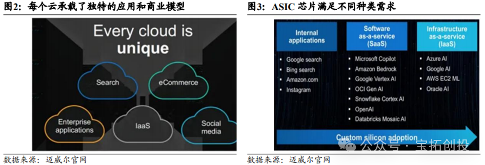
2. ASICs Can Adapt to Different Business Scenarios and Business Model Needs
Large cloud service providers’ business models and application scenarios are often carried by their own clouds, with each cloud hosting unique applications and business models, including internal applications (such as search engines, social media, etc.), SaaS services (such as AI chatbots, Copilot, etc.), and IaaS services. ASICs can adapt to the needs of different business scenarios and business models. ASICs can meet diverse customer needs, optimize internal workload architectures, achieve lower power consumption, lower costs, and provide memory and I/O architectures tailored for AI workloads.
3. Inference Power Demand Will Drive ASIC Market Space
As inference costs decrease, the demand for inference power is expected to continue to expand. AIGC models consume computational resources in proportion to the amount of input and output data, with costs calculated based on the number of tokens for input and output. For example, OpenAI’s API inference cost for GPT-4 in 2023 was $36 per million tokens, while the cost for GPT-4o in 2024 is expected to drop to $4 per million tokens, a decrease of 89%. 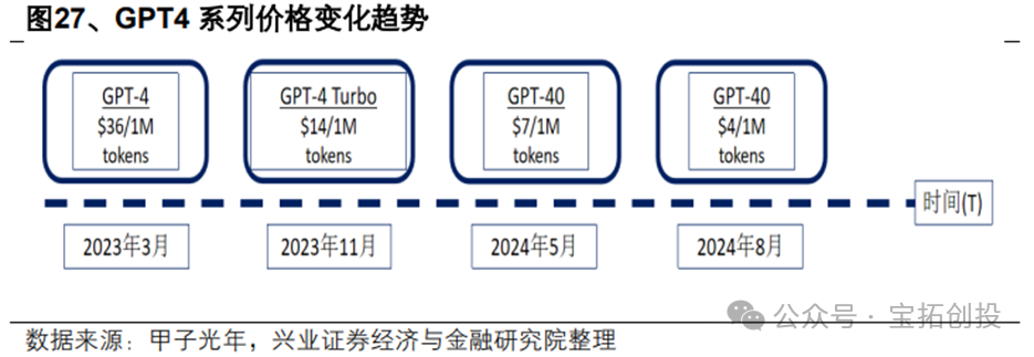 Deepseek accelerates the affordability of large models, significantly reducing the development costs of large models, driving a surge in demand for AI applications, and the demand for inference scenarios is increasing, shifting the computational demand from training to inference. IDC predicts that the proportion of inference server workloads in China is expected to increase from 65% in 2024 to 73% by 2028, showing an overall increasing trend in inference computing power.
 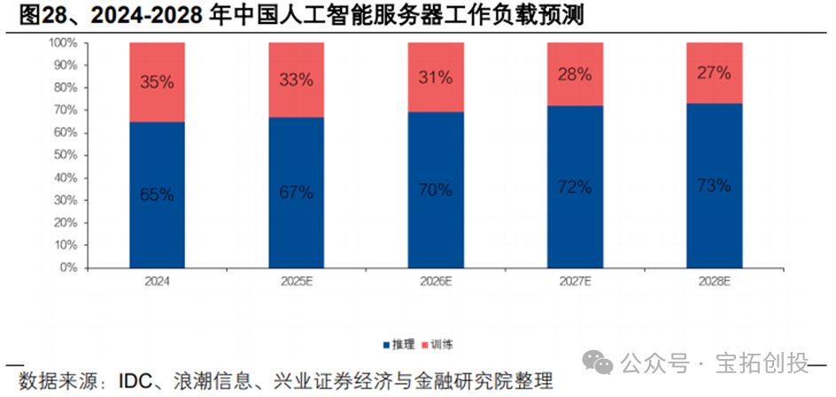 Inference chips focus more on power consumption, latency, and cost, with relatively lower accuracy requirements. ASIC chips have significant advantages in the inference field. According to CSET data, ASIC chips have clear advantages in inference, with their efficiency and speed being approximately 100-1000 times that of CPUs, and they possess significant competitiveness compared to GPUs and FPGAs. With the expected high growth in future inference demand, the market space is anticipated to grow rapidly.
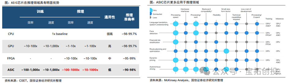
03
Market Participants
1. IP and Industry Chain Integration Are Major Challenges for Chip Self-Development, Requiring Support from External Manufacturers; Companies with Strong Comprehensive Capabilities Have Significant Competitive Advantages
The ASIC industry chain includes upstream design, midstream manufacturing, and downstream application segments such as cloud providers and large model customers. When system manufacturers self-develop AI ASIC chips, they typically collaborate with chip design manufacturers, and then the chips are manufactured by foundries like TSMC. The initial product launch from 0 to 1 usually requires more than two years of R&D. System manufacturers face high R&D costs and low first silicon success rates due to a lack of key IP and mass production experience. ASIC design companies can provide differentiated products for system customers, design high energy-efficient chips, significantly shorten design cycles, and reduce their own in-house R&D expenses. Considering that the cost of silicon wafers continues to rise with the iteration of advanced processes, ASIC design companies can leverage their rich design experience to help system manufacturers improve first silicon success rates, reducing time and R&D costs. The design process includes front-end design and back-end design flows. Front-end design mainly involves functional architecture design, including RTL programming simulation, logic synthesis, etc., while back-end design processes include layout planning, clock tree synthesis, timing optimization, physical verification, etc., before finally being sent to the foundry for silicon fabrication. American companies like Broadcom and Marvell have extensive and leading IP portfolios and high front-end design capabilities, allowing them to participate in deeper ASIC designs. The back-end design phase requires higher engineer experience, necessitating proficiency in the entire back-end process, tool usage, power consumption timing analysis, and simulation experience, represented by Taiwanese companies like Alchip and GUC. At the same time, ASIC design service companies maintain close cooperation with IP suppliers, EDA tool suppliers, and foundries. 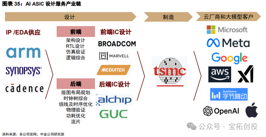 Broadcom Maintains Its Leading Position in the Industry with Rich Experience and a Leading IP Product Portfolio: 1) Experience and IP: Broadcom has over thirty years of experience in customized chips, developing its ASIC department through the combination of Avago, LSI, and HP, establishing an important position in networking and wireless fields through key IP and leading design capabilities, such as CPU, Serdes IP, connectivity IP, AD/DA converter IP, DSP processor IP, etc. Customized chips have evolved through more than 10 generations of technology, continuously advancing from 0.35μm to 3nm. 2) Downstream Synergy: Broadcom leads in market share in upstream components for cloud networking devices like switching chips, which is expected to create synergies with computing chips and routing chips to expand the AI product line. 3) Customer Relationships: The company has established a nearly ten-year partnership with Google, being the main manufacturer of Google’s self-developed TPU, making it the second-largest supplier in the AI chip field, only behind NVIDIA. Broadcom’s deployment of XPU (Broadcom’s term for AI ASIC) exceeded expectations in 26 years. In Q2 2025, Broadcom’s AI semiconductor revenue exceeded $4.4 billion, a year-on-year increase of 46%, marking nine consecutive quarters of growth. Customized AI accelerators (XPUs) achieved double-digit growth year-on-year, becoming one of the main components of AI semiconductor revenue. The company is advancing the deployment of customized AI accelerators with three customers and four potential customers, expecting at least three customers to deploy 1 million AI accelerator clusters each by 2027, with a “significant proportion being customized XPUs.” Customers are increasing investments due to rising inference demands, and XPU demand is expected to accelerate in the second half of 2026, continuing the growth trend of AI semiconductors into the 2026 fiscal year. Broadcom states that customized accelerators need to be co-developed with customers to enhance large language model (LLM) performance through “end-to-end optimization of hardware and software,” forming differentiated competitive advantages. Similarly, Marvell, as a leading global ASIC design manufacturer, has delivered over 2,000 customized ASICs in the past 25 years and is committed to developing key technologies and IP for the next generation of ASIC solutions. The company has fully leveraged its world-class 5nm and 3nm data infrastructure IP product portfolio, including industry-leading 112G XSR SerDes (serializer/deserializer), long-distance SerDes, PCIe Gen6/CXL3.0 SerDes, 240Tbps parallel chip interconnects, the latest Arm SoC processor subsystems, and low-cost/low-complexity packaging. Marvell’s leading XPU program for large U.S. hyperscale data center customers has performed outstandingly, becoming a key revenue driver for its customized business. The company is currently engaged in comprehensive cooperation with this customer for subsequent iterations, having secured 3nm wafer and advanced packaging capacity, with production expected to start in 2026. The architecture team is also supporting the definition of the next generation of products, reflecting the multi-generational advantages of long-term cooperation with Marvell. Revenue from customized AIXPUs for this customer is expected to continue to grow in FY2027 and beyond. Additionally, the joint development of a customized AIXPU project with another large U.S. hyperscale customer is progressing smoothly, with both parties coordinating on subsequent iteration architectures. Alchip Focuses on Back-End Design and Has Advanced Process Experience: Alchip focuses on fabless ASIC solutions, concentrating on back-end design services. The company has advantages in advanced process experience, achieving results in 7nm, 12nm, and 16nm process nodes. The company has a significant AI exposure, mainly due to early collaborations with U.S. CSP customers (such as Amazon and Intel), successfully launching AI training and inference chips like Trainium1, Inferentia1, and Inferentia2. However, due to a lack of IP technology, the company relies heavily on external procurement, resulting in significantly lower gross margins compared to U.S. ASIC design companies. GUC Provides Advanced Packaging Capabilities and TSMC Foundry Services: GUC focuses on back-end design services and possesses some self-developed IP capabilities such as HBM storage and UCIe interfaces. The company also maintains close cooperation with TSMC (TSMC is GUC’s largest shareholder) and advanced packaging companies, successfully achieving the silicon fabrication of ASIC chips based on TSMC’s 3nm and CoWoS technology, with rich IC design services and advanced process mass production experience.
2. The ASIC Market Shows High Growth Trends, with Domestic and Foreign Manufacturers Accelerating Layouts
The global market size for ASIC chips continues to grow, with a compound annual growth rate of 9.77% from 2019 to 2024. According to the Shenzhen Electronic Commerce Association and Verified Market data, the global ASIC market size is expected to reach $45.1 billion in 2024 (a year-on-year increase of 17.0%). In 2024, the global ASIC market is segmented by end application: consumer electronics (28%), telecommunications (20%), industrial (18%), automotive electronics (15%), aerospace and defense (10%), medical (5%), and others (5%). 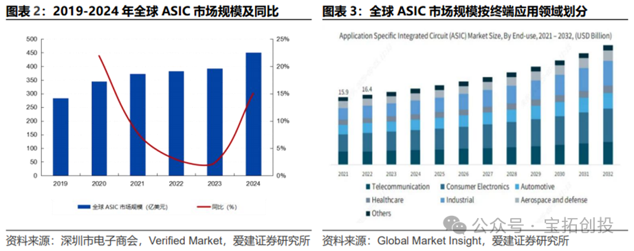 With the rapid popularization of emerging technologies such as artificial intelligence, 5G communication, and the Internet of Things, domestic and foreign manufacturers are accelerating their ASIC chip layouts. Google began considering ASIC layouts in 2006 and released its first TPU ASIC at the 2016 Google I/O conference, with subsequent iterations leading to the TPU V5P in 2023 and the V6e in 2024, maintaining a leading position with advanced processes and high computing power; Amazon released Trainium in 2023 and Trainium2 in 2024, focusing on cloud energy efficiency optimization; and Microsoft has released the Maia 100 and Meta has launched the MTIA series, among others. Domestic manufacturers, including Huawei Ascend (designed by HiSilicon) and Cambricon, are also designing chips based on ASIC architecture.
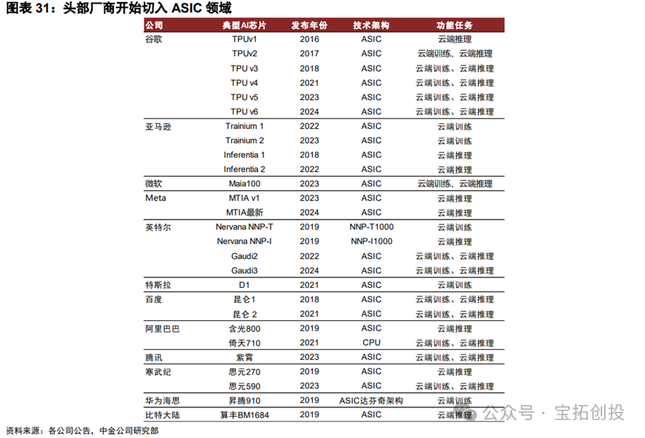
04
ASIC Architecture and Ecosystem
ASIC architecture and ecosystem are vastly different, becoming a strong complement to GPUs. 1) There are differences between ASIC and GPU architectures: GPUs are based on general-purpose parallel computing transitioning to AI, with internal designs typically consisting of numerous parallel computing cores and small AI acceleration units (Tensor Cores); TPUs, on the other hand, are designed directly for AI computing needs, with representative architectures such as large pulse arrays. 2) There are differences in development ecosystems: NVIDIA has a complete and mature CUDA development ecosystem, while AMD’s GPU/ASIC manufacturer development ecosystem is not yet complete.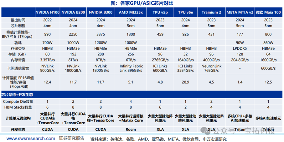
1. ASIC Architecture: Custom Architectures Based on Pulse Arrays Are an Important Route
GPUs are based on the von Neumann architecture, requiring high-frequency data exchange with registers during computations, which demands high storage capacity. GPUs are primarily designed for data-parallel execution, with a small control unit and numerous execution units, along with a large number of register files to hide latency across multiple execution threads. Google’s TPU and AWS’s Tranium2 are both based on pulse array architectures, specifically designed for matrix computations, allowing computation results to be directly passed to the next computation unit until the matrix results for that dimension are fully computed, reducing unnecessary global data exchanges. 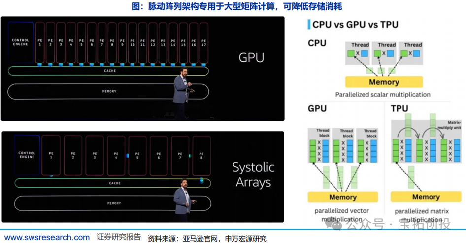
2. ASIC Development Ecosystem
(1) Google and AWS Both Use Pulse Arrays + XLA
The development ecosystem should gradually mature in the direction of improving ROI in hardware architecture/computational architecture, with domestic AI computing power and overseas cloud provider ASIC chips both having potential. DeepSeek has proven to have a strong engineering team capable of building a relatively usable development ecosystem for other AI chips (though ease of development is still expected to have significant gaps). XLA is a compiler built by Google for TPU, which has gradually combined with AI frameworks like JAX to form a development ecosystem that is maturing. AWS’s Tranium2, also based on pulse array architecture, similarly adopts XLA, accelerating related ecosystem updates and iterations. 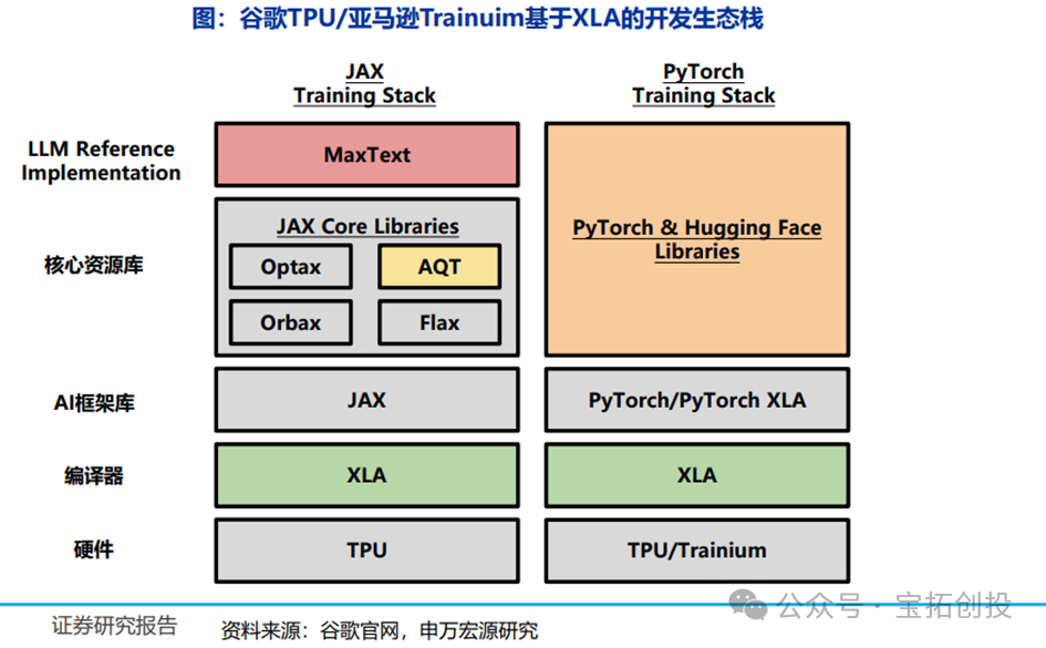
(2) META MTIA V2 Software Stack Based on Triton
Triton is an open-source programming language similar to Python launched by OpenAI in July 2021, aimed at reducing the programming difficulty of GPUs, but Triton does not heavily rely on a single vendor’s GPU and can be extended to non-GPU hardware architectures like MTIA V2. Pytorch is working to promote Triton, which has achieved high hardware efficiency on NVIDIA GPUs without CUDA. MTIA V2 is based on Triton and provides a Triton-MTIA compiler to further optimize the software stack. 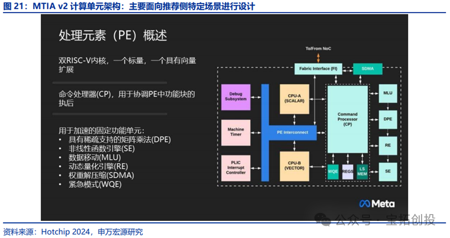
3. ASIC Costs: Cost-Effective but Relatively Limited in Use
Simple calculations of the manufacturing costs of various chips are mainly based on the specific storage capacity, wafer size, etc., and estimated based on the gross margins of NVIDIA, Broadcom, Marvell/AIChip. ASIC chips are indeed cost-effective in specific task deployments, but are limited by the development ecosystem: 1) During the development process, the immature ecosystem leads to efficiency losses, which increases hidden costs to some extent. 2) The scenarios are limited to internal loads of cloud providers, making it relatively difficult for cloud customers to develop. 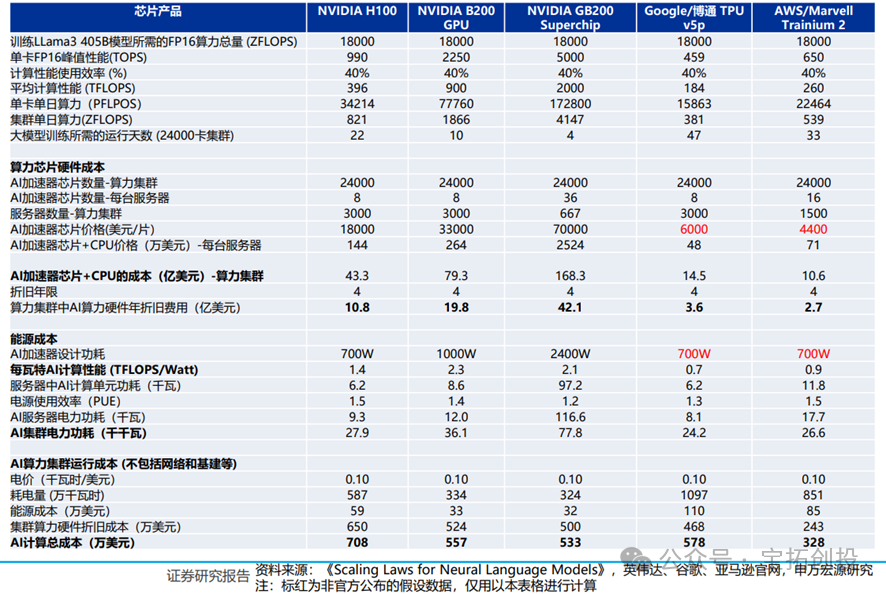 Typical training scenarios are cost-effective:
05
Overseas Cloud ProvidersASIC Layout Situation
1. Google: Google Customizes ASICs Specifically for AI
Google’s TPU (Tensor Processing Unit) is a custom ASIC chip designed specifically to accelerate machine learning tasks, primarily used for deep learning training and inference. The TPU is essentially a computing core specifically for matrix multiplication, connected to high-bandwidth memory (HBM); the basic components of the TPU include matrix multiplication units (MXUs), vector units (VPUs), and vector memory (VMEM); the matrix multiplication unit is the core of the TensorCore, while the vector processing unit performs general mathematical operations, and the vector memory is an on-chip cache located close to the computing units; TPUs are extremely fast at performing matrix multiplications. 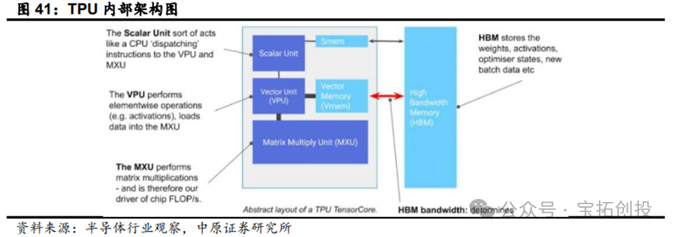 Currently, Google’s TPU has iterated to its seventh generation, with each generation showing certain improvements in chip architecture and performance compared to the previous generation: In 2015, Google launched TPU v1, primarily for inference tasks. In 2024, Google released the sixth-generation product TPU v6 Trillium, which improved peak computing performance per chip by 4.7 times compared to the previous generation TPU v5e, doubling both HBM capacity and bandwidth, while also doubling the inter-chip interconnect bandwidth; TPU v6 Trillium has significantly reduced operational costs with a 67% improvement in energy efficiency compared to the previous generation; TPU v6 Trillium is used to train Google’s Gemini 2.0 and other large AI models.
  Google’s TPU iterations have significantly improved the efficiency of training and inference for large models. Large AI models like Gemini are powerful and complex, with billions of parameters, requiring immense computational power and jointly designed software optimizations for training such dense models. Compared to the previous generation TPU v5e, TPU v6 Trillium provides up to 4 times the training speed for large models like Llama-2-70b and gpt3-175b. TPU v6 Trillium has made significant improvements for inference workloads, providing the best TPU inference performance for image diffusion and large models, enabling faster and more efficient AI model deployment; compared to TPU v5e, TPU v6 Trillium’s offline inference throughput for Stable Diffusion XL is 3.1 times higher, and server inference throughput is 2.9 times higher.
  TPU v6 Trillium is expected to largely replace the existing TPU v5 by 2025. In the development of the new generation of products, Google has changed its previous single-supplier model of only collaborating with Broadcom (Broadcom) to include cooperation with MediaTek, forming a dual-supplier layout. This move not only enhances design flexibility and reduces reliance on a single supply chain but also helps strengthen its layout in advanced process fields. Google has established a computing power cluster of 100,000 TPU chips. TPU chips are connected into computing power clusters through ICI, and the TPU network can connect 16x16x16 TPU v4 and 16x20x28 TPU v5p. To meet the growing demand for AI computing, Google has connected over 100,000 TPU v6 Trillium chips into a network structure, creating one of the world’s most powerful AI supercomputers; this system combines over 100,000 TPU v6 Trillium chips with the Jupiter network structure, which has a bandwidth of 13PB per second, allowing a single distributed training job to scale across hundreds of thousands of accelerators. This large-scale chip cluster can provide powerful computing capabilities, enabling efficient parallel computing, thereby accelerating the training process of large models and improving the performance and efficiency of AI systems.
  In April 2025, the seventh-generation TPU, Ironwood, was officially launched, designed for the large-scale deployment of thinking and inference AI models, marking a significant shift in the infrastructure supporting AI development from providing real-time information for human interpretation to generating and interpreting proactive insights. In terms of core computing performance, it breaks barriers with a maximum of 42.5 exaflops of computing power. Each individual Ironwood chip provides a peak computing capability of 4614 TFLOPs. A cluster of 9216 TPUs has a total computing power of 42.5 Exaflops, which is more than 24 times the computing power of the world’s largest supercomputer, El Capitan (which provides 1.7 Exaflops per cluster).
  Ironwood has made significant upgrades in its memory subsystem. In terms of single-chip specifications, Ironwood significantly enhances memory and bandwidth, with each chip equipped with 192GB of high-bandwidth memory (HBM), which is six times that of the previous generation TPU Trillium. Each chip’s memory bandwidth reaches 7.2 terabits/s, which is 4.5 times that of Trillium. The larger memory capacity allows for caching larger model parameters and longer context information locally on the chip, reducing access to external storage; the higher bandwidth enables faster feeding of data to computing units, both of which directly contribute to reducing inference latency and improving the efficiency of processing complex models. Ironwood also significantly enhances computing efficiency, with its performance per watt being twice that of Trillium and nearly 30 times higher than the first TPU launched in 2018. In the context of data center energy consumption becoming a bottleneck and a major operational cost, the improvement in energy efficiency is of significant value for the sustainable development and large-scale economic deployment of AI technology. Google also emphasizes its advanced liquid cooling technology, aimed at ensuring that chips can operate stably and efficiently under high loads.
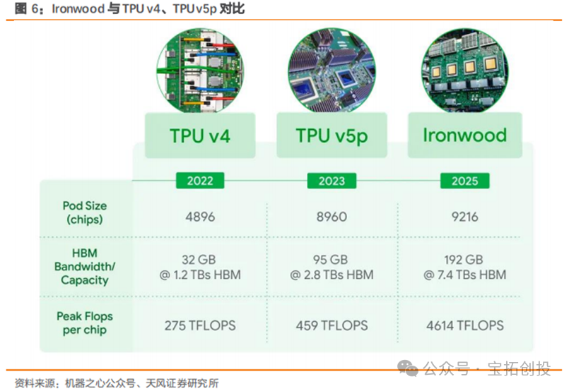 According to Google, the significantly enhanced performance of Ironwood is designed to meet the diverse computational needs required by thinking models. In cutting-edge fields, the computational demands of thinking models far exceed the capabilities of any single chip. Therefore, Ironwood TPU features low latency and high bandwidth ICI networks to support coordinated and synchronized communication at the scale of TPU units. Google also emphasizes that Ironwood will be used in conjunction with its machine learning runtime, Pathways, allowing developers to easily leverage the combined computational power of thousands of Ironwood TPUs. For enterprise customers, Ironwood will offer two configurations: a 256-chip configuration and a 9,216-chip configuration.
2. Meta: Self-Developed ASIC Chips for Dedicated Loads, Helping to Reduce Costs and Increase Efficiency
Meta’s core computing power load comes from recommendation system scenarios, providing a fertile ground for self-developed ASIC chips emphasizing specialization. In Meta’s business, the video/ad recommendation system is the main source of computing power workload, and the continuously upgraded recommendation system is still increasing the demand for computing power. Developing more specialized ASIC chips for this specific area, compared to completely outsourcing general-purpose computing chips, is expected to bring cost optimization advantages. Meta launched the MTIA V1 and MTIA V2 chips in May 2023 and April 2024, respectively. The initial MTIA chip, manufactured using TSMC’s 7nm process, achieves a computing power (INT8) of 102 TFLOPS with a power consumption of 25 watts. From MTIA V1 to MTIA V2, Meta’s self-developed chips have shown significant improvements in performance and efficiency. MTIA V2, based on TSMC’s 5nm process, can handle low-complexity (LC) and high-complexity (HC) ranking and recommendation models, improving the following aspects: 1) Memory: MTIA V2 adopts an 8×8 processing element (PE) layout, with single PE storage performance reaching 384KB, which is a 2x improvement over MTIA V1; 2) Processing Capability: MTIA V2 chips have higher computing power, achieving 354 TFLOPS/177 TFLOPS under INT8/FP16 precision, a 3.5x performance improvement over MTIA V1; 3) Transmission Efficiency: MTIA V2 chips have more efficient data transmission, with 8 PCIe Gen5 interfaces providing a maximum transmission efficiency of 32GB/s, a 2x improvement over MTIA V1. 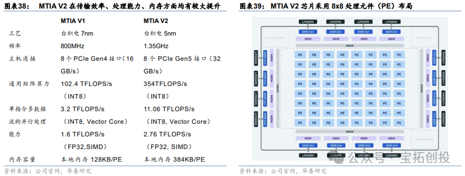 MTIA V2 aims to efficiently serve ranking and recommendation models, providing users with high-quality recommendations. MTIA V2 is primarily designed to meet the computing power demands brought by Meta’s increasingly evolving recommendation engine. From a design perspective, the PE (Processing Element) is the main computing unit of the entire MTIA V2. This includes conventional computing cores and numerous cores optimized for specific calculations. In addition to one CPU unit for scalar calculations and one for vector calculations, multiple types of acceleration units have been designed through a command processor. These include dynamic quantization engines (RE), enhanced data movement units (MLU), units supporting nonlinear function calculations (SE), and matrix multiplication units emphasizing sparse support (DPE), specifically optimized for the calculations of recommendation systems. The numerous targeted designs allow MTIA V2 to reduce storage and bandwidth consumption when processing large-scale data, thereby enhancing overall computing performance. These features are crucial for recommendation engines, as they often need to handle large amounts of complex data tables and weights.Meta plans to launch the MTIA V3 chip in 2026, which is expected to be equipped with high-end HBM. Unlike the V1/V2 chips, which focus on specific tasks such as advertising and social networking, it is expected to expand applications to model training and inference tasks.
3. Amazon AWS: Continuously Iterating the Trainium Series AI Chips, Benefiting from Computing Power Infrastructure
AWS (Amazon Web Services) has laid out its AI chip strategy mainly around inference chips (Inferentia) and training chips (Trainium). Since 2020, Amazon has released two generations of Trainium chips. The Trainium1 accelerator provides 190 TFLOPS of FP16/BF16 computing power, equipped with 32GB of HBM and a memory bandwidth of 820GB/s; the AWS Trainium2 chip’s performance is up to 4 times better than the first generation Trainium. The Amazon EC2 Trn2 instance, based on Trainium2, is built specifically for generative AI and is the most powerful EC2 instance for training and deploying models with hundreds of billions to trillions of parameters. The price-performance ratio of Trn2 instances is 30-40% better than the current generation GPU-based EC2 P5e and P5en instances. The Trn2 instance is equipped with 16 Trainium2 chips, which are interconnected via NeuronLink. The Trn2 UltraServer is a new EC2 product that is very suitable for the largest models that require more memory and memory bandwidth than independent EC2 instances can provide. The UltraServer design uses NeuronLink to connect 64 Trainium2 chips across four Trn2 instances to a single node. For inference, the UltraServer can help provide industry-leading response times, creating the best real-time experience. For training, compared to independent instances, UltraServers improve model training speed and efficiency through faster collaborative communication, enhancing model parallelism. NeuronCore-v3 is the third-generation NeuronCore driving the Trainium2 chip. It is a fully independent heterogeneous computing unit composed of four main engines: Tensor engine, Vector engine, Scalar engine, and GPSIMD general-purpose programmable engine, with on-chip software-managed SRAM memory to maximize data locality and optimize data prefetching. 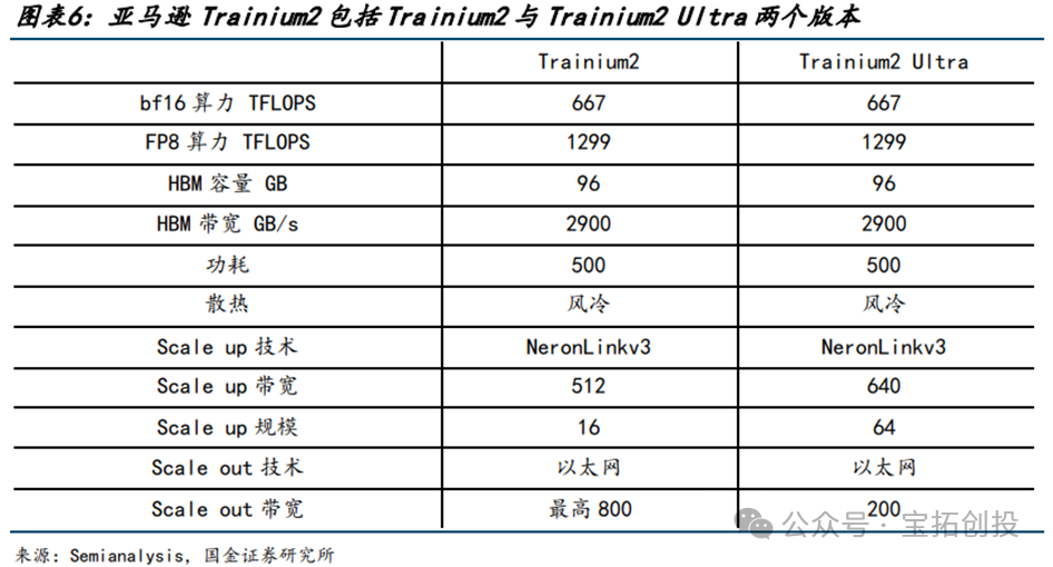 AWS plans to release the next generation of AI semiconductors, Trainium3, later this year, using a 3nm process and manufactured by TSMC. Trainium3’s performance is expected to double compared to the previous generation, with a 40% improvement in energy efficiency, and the performance of UltraServers equipped with this chip is expected to increase fourfold. The release of Trainium3 further consolidates Amazon’s advantage in the integration of cloud services and AI chips, providing customers with higher performance and lower-cost AI solutions. In 2018, Amazon announced the development of chips optimized for AI inference, Inferentia, focusing on reducing the cost of running large-scale deep learning models. The company launched Inferentia2 in 2023, the second-generation AWS dedicated machine learning inference accelerator, with each chip featuring two NeuronCore-v2 cores. Inferentia2 can provide up to 380 TFLOPS for INT8 data types and 190 TFLOPS for FP16/BF16 data types, with additional support for FP32, TF32, and configurable FP8 (cFP8) data types. In terms of memory, Inferentia2 has 32GB of HBM with a bandwidth of 820GB/s, increasing total memory by 4 times and memory bandwidth by 10 times compared to Inferentia.
 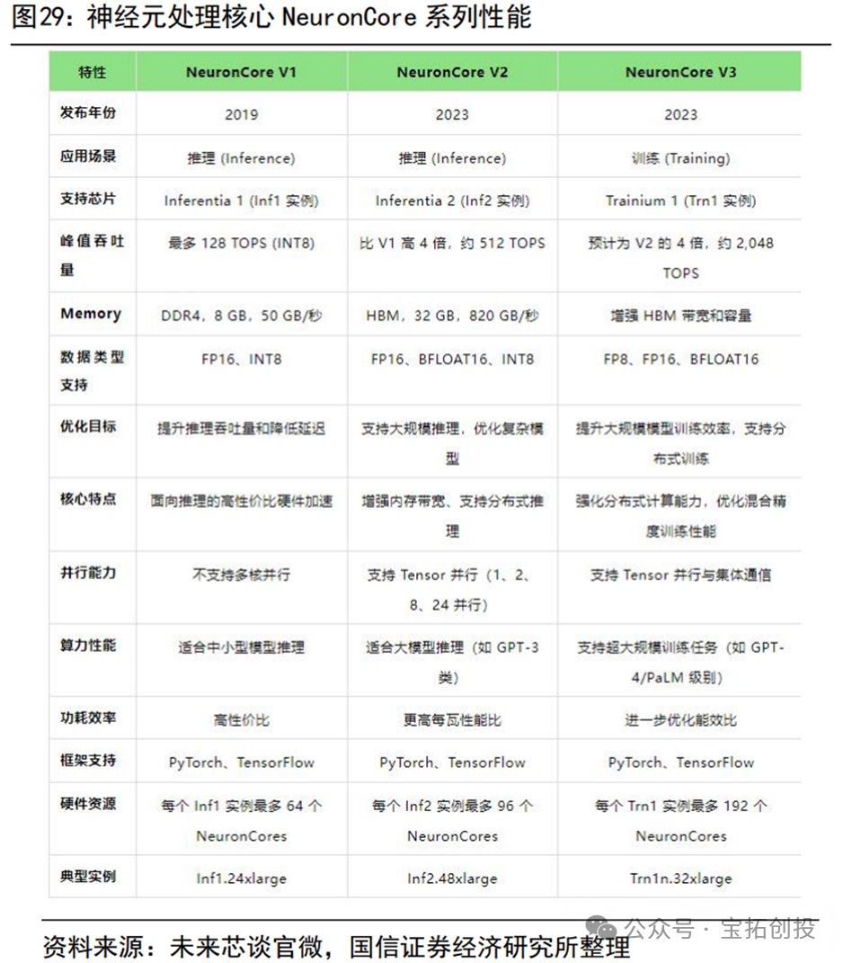 Currently, companies including Adobe, AI startup Poolside, data platform service Databricks, and Qualcomm are using Trainium2 processors to train their AI models, with Qualcomm processing AI models in the cloud before transferring them to the edge. Apple is also utilizing services provided by Amazon’s ASIC chips for Siri, Apple Maps, and Apple Music. Apple uses Amazon’s Inferentia and Graviton chips to support its search services.
4. Microsoft: Self-Developed Chip Maia 100
Microsoft has developed Maia 100 as a custom AI accelerator for running OpenAI’s models and AI workloads like Copilot on Azure. Maia 100 uses TSMC’s 5nm process and CoWoS-S packaging technology, equipped with 64GB (4×16GB) of HBM2E, with a memory bandwidth of 1.8TB/s. Maia 100 achieves performance of 3200 TFLOPS under MXFP4 data format, 1600 TFLOPS under Int8, and 800 TFLOPS under BF16, exceeding NVIDIA A100 performance by 28% and H100 performance by 40%. Microsoft’s Maia 100 single SoC is equipped with 16 clusters, each containing 4 tiles. Maia 100 has image decoding and confidential computing capabilities, supporting a wide range of data types, including FP32 and BF16. 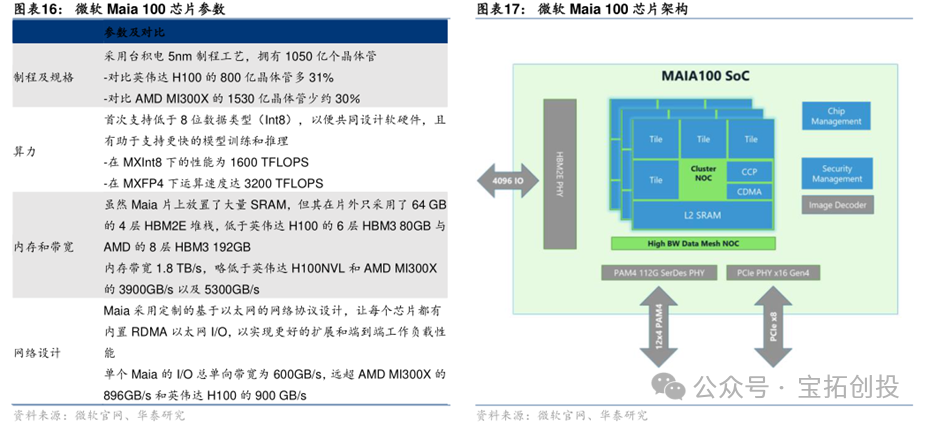 Maia 100 is based on a custom RoCE-like protocol and Ethernet interconnect, with a built-in AES-GCM encryption engine to protect user data, achieving a network connection bandwidth of 600GB/s. Maia 100 is also supported by a unified back-end network for workload scaling and horizontal expansion, providing flexibility for direct and switch connections. The Ares rack for Microsoft’s Maia 100 is equipped with 32 Maia 100 chips. Each Ares rack contains 8 servers, each with 4 Maia 100 chips, totaling 32 Maia 100 chips per rack. The Ares rack can reach a power capacity of 40kW, equipped with a Sidekick liquid cooling system, with auxiliary devices set on both sides of the rack, where cold liquid flows from the auxiliary devices to the cold plates on the Maia 100 surface, absorbing heat from the liquid before outputting the cold liquid, thus creating a cooling cycle.
 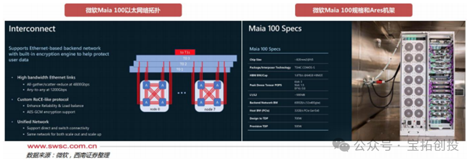 The design for the next-generation Maia v2 has been confirmed, with back-end design and mass production delivery handled by GUC. In addition to deepening cooperation with GUC, Microsoft has also involved MediaTek in the design and development of the Maia v2 upgrade to strengthen its self-developed chip technology layout and effectively disperse technical and supply chain risks during the development process. Maia SDK Enables Rapid Deployment and Model Portability. Microsoft has created software for Maia 100 that integrates with popular open-source frameworks like PyTorch and ONNX Runtime. This software stack provides a rich and comprehensive library, compiler, and tools, enabling data scientists and developers to successfully run models on Maia 100. Microsoft has integrated OpenAI’s Triton; the Maia SDK allows users to quickly port models written in PyTorch and Triton to Maia.
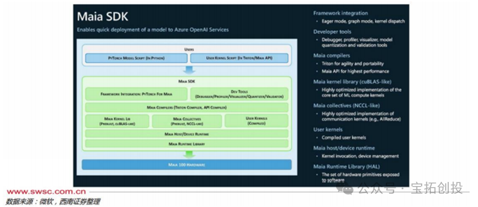
06
Related Companies
Domestically, companies like Chipone and Aojie Technology have strong competitiveness in ASIC design. Domestic chips are accelerating their catch-up, with companies like Huawei HiSilicon, Cambricon, and Haiguang Information becoming industry leaders. Huawei’s Ascend series processors have achieved significant breakthroughs in technology and application since their inception, especially with the release of Ascend 910B in 2023. Cambricon’s flagship product, MLU590, is set to launch in June 2024, focusing on AI training and inference. Another important product from Cambricon, MLU370-X4, is expected to launch in November 2024, focusing on providing more cost-effective AI acceleration solutions. Haiguang Information is also gradually becoming an important player in the domestic AI chip market, with core products including Deep Calculation No. 1, Deep Calculation No. 2, and the upcoming Deep Calculation No. 3. 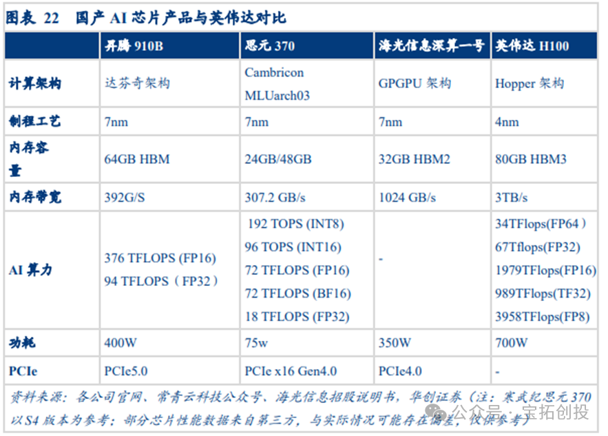
1. Aojie Technology
Aojie Technology is a leading domestic baseband SoC manufacturer. The company is a platform chip enterprise providing wireless communication and ultra-large-scale chips. Since its establishment, the company has focused on the R&D and technological innovation of wireless communication chips, possessing the R&D and design capabilities for full-standard cellular baseband chips and multi-protocol non-cellular IoT chips, as well as the ability to provide ultra-large-scale high-speed SoC chip customization and semiconductor IP licensing services. The company’s cellular baseband chip products cover the 2G/3G/4G/5G fields; in the non-cellular mobile communication field, the company not only has various high-performance non-cellular networking chips based on WiFi, LoRa, and Bluetooth technologies but also global positioning and navigation chips based on Beidou Navigation (BDS)/GPS/Glonass/Galileo technologies. In the field of ultra-large-scale high-speed SoC chip design and semiconductor IP licensing services, based on recognition of the company’s technical team’s rich chip design experience and strong technical accumulation, customers such as S, Denglin Technology, U.S. Moffett, OPPO, and Xiaomi have selected the company to provide chip design services or IP licensing. 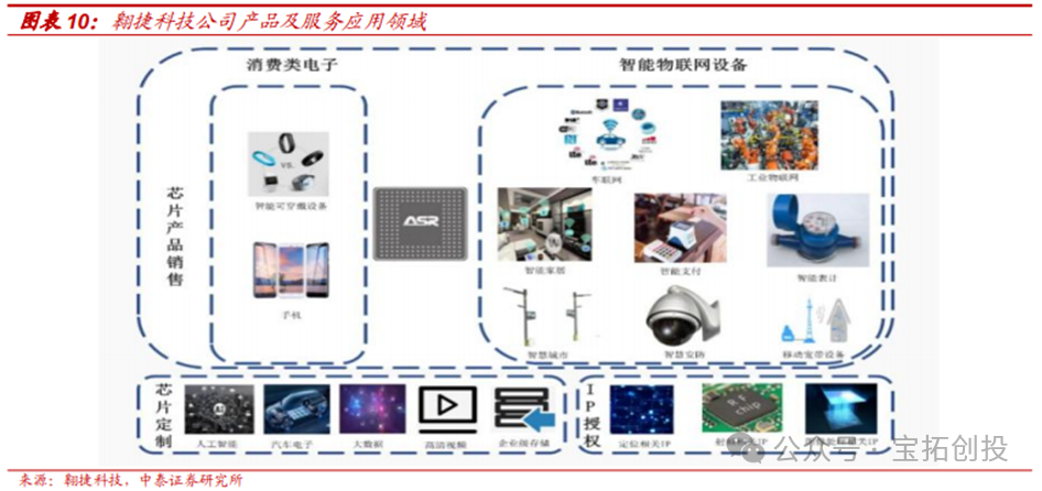 The company released its 2024 annual report, achieving revenue of 3.386 billion RMB in 2024, a year-on-year increase of 30.23%; achieving a net profit attributable to the parent company of -693 million RMB, a year-on-year decrease of 37.01%, and a net profit attributable to the parent company after deducting non-recurring gains and losses of -707 million RMB, a year-on-year decrease of 7.38%. In Q4 2024, the company achieved revenue of 846 million RMB, a year-on-year increase of 11.94%, with a net profit attributable to the parent company of -281 million RMB, a year-on-year decrease of 252.9%. The company’s chip products, chip customization business, and semiconductor IP licensing accounted for 89.02%, 9.92%, and 1.04% of its main business revenue, respectively. The chip customization business has seen high growth, achieving revenue of 336 million RMB in 2024, a year-on-year increase of 48.38%. IP licensing revenue was 35 million RMB.
2. Chipone
Chipone is a leading domestic semiconductor IP supplier, with multiple processor IPs including GPU IP and NPU IP, capable of providing one-stop chip customization services for customers. The company’s chip design capabilities cover 14nm/10nm/7nm/5nm FinFET and 28nm/22nm FD-SOI, enabling it to provide system solutions from hardware to software. In March 2023, Lanyan Intelligent released a high-performance AI chip based on the Chiplet architecture developed in collaboration with Chipone, with the chip’s computing power reaching 8 TFLOPS with Chipone’s GPGPU IP and 240 TOPS with Chipone’s NPU IP. Currently, chips with Chipone’s GPU IP have shipped nearly 2 billion units globally, and Chipone’s NPU IP has been used by 72 customers in 128 AI chip designs, with over 100 million units shipped globally. The company is actively developing high-performance graphics processor technology aimed at data centers and GPU AI computing, supporting 16-32 TFLOPs FP32 computing power, 128-1536 Texel/cycle texture processing capability, and 32-384 Pixel/cycle pixel fill capability. As a top ASIC design company in China, Chipone demonstrates its strong ASIC R&D capabilities in various aspects. In 2024, the company achieved total operating revenue of 2.322 billion RMB, a year-on-year decrease of 0.69%; achieved a net profit attributable to the parent company of -601 million RMB; achieved a net profit attributable to the parent company after deducting non-recurring gains and losses of -643 million RMB. As of 2024, the company has a research and development team of 1,800 people, including many senior experts from internationally renowned companies such as Broadcom and Marvell, laying a solid foundation for its technological breakthroughs. In terms of IP capabilities, the chip IPs laid out by Chipone, including GPU, NPU, and VPU, serve many globally renowned companies, with IP licensing revenue reaching 736 million RMB in 2024. In terms of ASIC capabilities, Chipone’s design capabilities range from 5nm FinFET and 22nm FD-SOI to traditional 250nm CMOS processes, serving well-known companies like Intel, Amazon, Google, and Microsoft, with chip customization revenue reaching 1.581 billion RMB in 2024.
3. Huawei Ascend
Ascend 910B 7nm Process Empowers Strong Computing Power, Multi-Card Interconnection Supports Large-Scale Computing. Huawei’s Ascend 910B adopts an advanced 7nm process, optimizing power consumption and enhancing computing power density, supporting large-scale AI training tasks, particularly excelling in floating-point operations and large-scale parallel computing. Its FP16 computing power reaches 376 TFLOPS, making it very suitable for compute-intensive tasks such as deep learning and big data analysis. The Ascend 910B is equipped with 64GB of HBM2e memory, with a memory bandwidth of around 400GB/s, greatly enhancing data processing capabilities and effectively reducing data bottlenecks, ensuring training efficiency for large datasets. The maximum design power consumption of Ascend 910B is only 400W, demonstrating its excellent energy efficiency. In multi-card parallel computing, Ascend 910B supports an 8-card HCCS interconnection scheme, which, supported by a bandwidth of 393GB/s, through efficient inter-card interconnection technology (HCCS), not only meets the high-performance requirements of a single card but also fully unleashes its computing power during multi-card parallel computing, providing stable performance for large-scale computing. 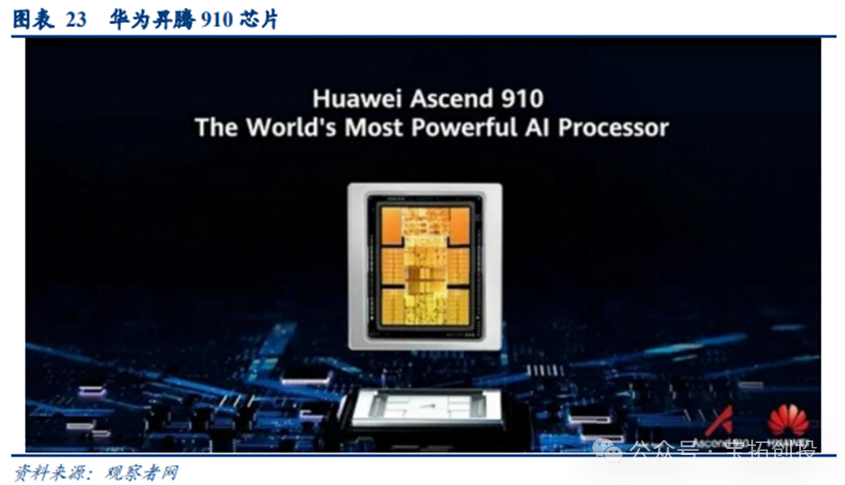
4. Cambricon
Cambricon Continues to Deepen Its AI Chip Field, Constantly Innovating and Breaking Through Technologically. As a leader in the domestic AI chip design field, Cambricon’s market competitiveness in inference computing and AI acceleration for edge devices is increasingly prominent. In June 2024, Cambricon will launch its flagship product, MLU590, focusing on AI training and inference. According to data from the Northern Computing Network public account, this chip is built on a 7nm process, with FP16 computing power of 314 TFLOPS and equipped with 80GB of memory, with a memory bandwidth of up to 2048GB/s. This configuration allows MLU590 to perform excellently in high-performance computing and deep learning training, easily handling large-scale data processing tasks. Its maximum design power consumption is 350W, suitable for high-density computing scenarios. Meanwhile, with an interconnect bandwidth of up to 318.8GB/s, it supports efficient multi-card parallel computing, further strengthening its capabilities in large-scale AI computing. To meet more diverse market demands, Cambricon will launch MLU370-X4 in November 2024, focusing on cost-effective AI acceleration solutions. Compared to MLU590, its FP16 computing power is 96 TFLOPS, equipped with 24GB of LPDDR5 memory, with a memory bandwidth of 307.2GB/s and a maximum design power consumption of 150W. This new product provides a new option for mid-to-low-end AI inference tasks while maintaining Cambricon’s technological advantages, broadening the application scenarios of Cambricon’s products. 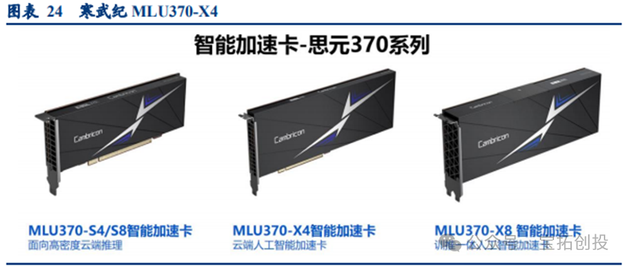
5. Haiguang Information
Haiguang Information is Gradually Becoming an Important Player in the Domestic AI Chip Market, with Core Products Including Deep Calculation No. 2 and the Upcoming Deep Calculation No. 3. These products mainly serve the AI inference and small-scale training markets, widely used in cloud computing, data centers, and AI acceleration computing fields. According to reports from the Securities Market Weekly, the Deep Calculation No. 2 launched in 2023 is an acceleration card aimed at small-scale AI training and inference, adopting a 7nm FinFET process, with FP16 computing power of 49 TFLOPS and FP32 computing power of 23 TFLOPS, suitable for inference tasks in low-power devices. This product marks Haiguang Information’s initial layout in the AI inference market, showcasing strong cost-effectiveness. Additionally, Deep Calculation No. 3 is expected to have significant computing power improvements and may surpass international competitors like NVIDIA’s A800 in the AI inference field, especially in inference and high-precision computing tasks. Haiguang Information’s DCU series is based on GPGPU architecture, compatible with general “CUDA-like” environments, and can adapt to mainstream international commercial computing software and AI software. The design of DCU focuses on high parallel computing capabilities, making it particularly suitable for handling the large data throughput demands in AI inference tasks. 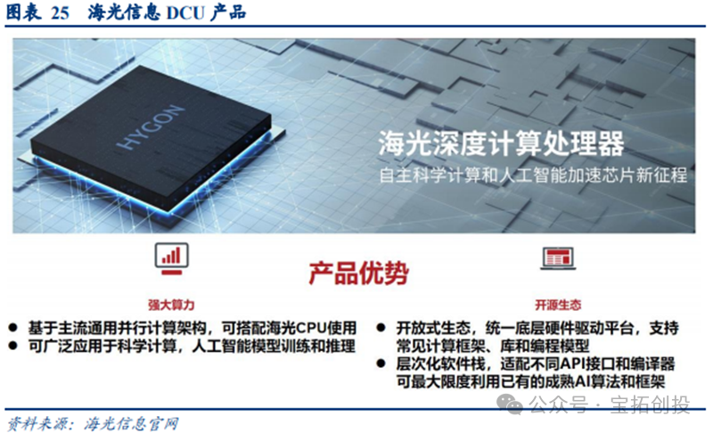
6. Domestic Internet Giants
Domestic Internet giants are actively laying out self-developed ASIC chips, achieving remarkable results. Tencent initiated the development of the Canghai codec chip in early 2019, which was mass-produced and put into use in 2022, providing services for cloud gaming, direct streaming, and other scenarios. In 2022, it launched the Zixiao AI inference chip, which adopts a self-developed architecture and acceleration module, significantly improving computing acceleration performance and reducing costs; it also supports cloud computing virtualization with zero loss through the Xuanling high-performance network chip. According to reports from The Paper, Alibaba released the Lingguang 800 AI inference chip in 2019, with computing power equivalent to 10 traditional GPUs and an energy efficiency ratio 3.3 times that of the second place, applied in fields such as smart cities and intelligent security; in 2021, it launched the Yitian 710 general-purpose server chip, manufactured using a 5nm process, providing computing power support for Alibaba Cloud servers. ByteDance has not officially announced its self-developed chip achievements but may increase self-developed investments. Baidu launched China’s first cloud-based fully functional AI chip, Kunlun 1, in 2018, with over 20,000 units deployed; in 2021, it mass-produced Kunlun 2, using a 7nm process, with performance improvements of 2-3 times, suitable for multiple scenarios including cloud, edge, and on-device. 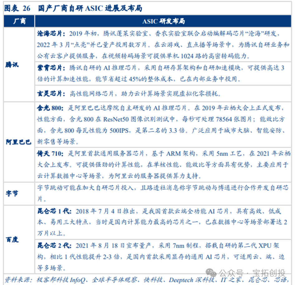
07
Applications and Scale Forecasts of ASICs
According to Cervicorn Consulting, the global data center market size is expected to reach $217.65 billion in 2024. In the AI inference phase of data centers, the importance of ASICs is increasingly prominent. In 2017, ASICs accounted for only 10% of the data center chip market, and this is expected to rise to 40% by 2025. ASICs are customized for AI algorithms, improving efficiency and reducing power consumption, significantly driving the development of AI inference, and have become an indispensable part of data centers. 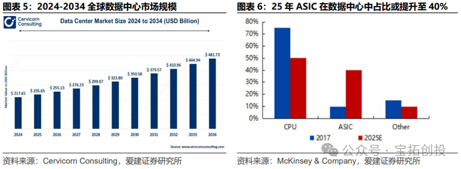 While data centers focus on the centralized analysis and storage of large-scale data, edge computing focuses on addressing the computational needs of real-time scenarios, with both functions complementing each other. In edge computing, the choice of chips directly affects data processing efficiency, latency, and energy consumption. Among them, ASIC chips are increasingly prominent in the edge computing AI inference chip market. From 2017 to 2025, the share of ASICs is expected to rise from 50% to 70%, while CPUs will drop from 50% to 0%, and FPGAs are expected to rise from 0% to 20%.
 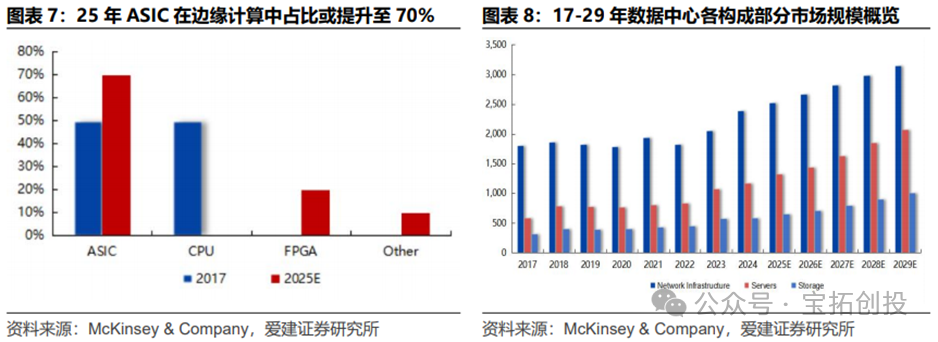 The composition of data centers includes network infrastructure, servers, and storage, with servers being a crucial component of data centers. The global server market size is expected to reach $117.3 billion in 2024 (a year-on-year increase of 8.6%); the market size of servers in China is expected to reach 245.6 billion RMB in 2024 (a year-on-year increase of 10.1%), becoming the core driving force for global data center growth. Accelerated servers are a key component of server systems, significantly enhancing the efficiency of AI training/inference and high-performance computing scenarios by integrating dedicated acceleration chips such as GPUs, ASICs, and FPGAs, and have become the core hardware for data centers to cope with explosive computing power demands.
 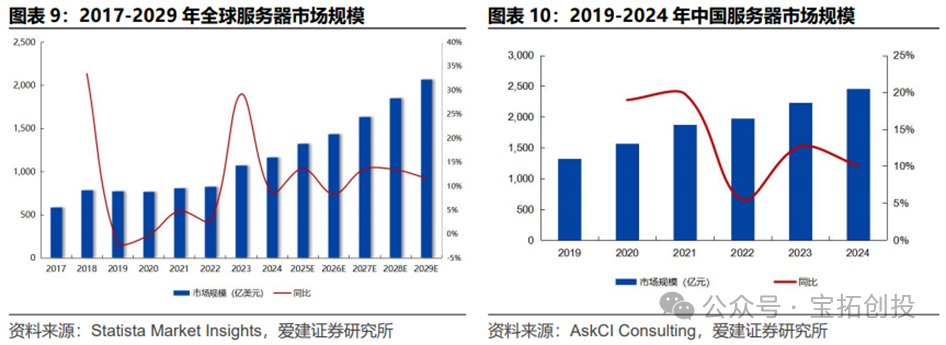 IDC data shows that the market size of accelerated servers in China is expected to reach $22.1 billion in 2024 (a year-on-year increase of 134%), with GPU servers accounting for 69% and ASIC/FPGA and other non-GPU accelerated servers accounting for over 30%. The market size is expected to exceed $55 billion by 2028, with ASIC accelerated servers accounting for nearly 40%.
08
References Research Reports
1. Industrial Securities – Electronic Industry Mid-Term Strategy 2025: Seize AI Innovation and Localization, Grasp Strategic Heights2. Zhongyuan Securities – Semiconductor Industry: AI Computing Power Chips Are the “Engine of the AI Era”, Henan Province Focuses on Layout3. Minsheng Securities – Electronic Industry In-Depth Report: Computing Power Equality, Rise of Domestic AI Forces4. Guoxin Securities – ASIC Industry Commentary: The Law of Customization, Focus on Domestic ASIC Service Providers5. CICC – MediaTek -2454.TT – Both Offense and Defense, SoC Chip Leader Fully Layouts AI6. Aijian Securities – Electronic Industry Weekly: ASIC Becomes a New Windfall in the Server Chip Field7. Tianfeng Securities – Consumer Electronics Industry: Apple Supply Chain Valuation at Relatively Low Levels, Suggesting Attention to Opportunities for Upstream Recovery8. Huatai Securities – Google – GOOGL.US – The Search King at a Crossroads, Can It Regain AI Dominance?9. Huatai Securities – Internet Industry: Tech Giants’ Capex Enthusiasm Remains High, but Market Expectations Shift to Actual Performance10. Guojin Securities – Electronic Industry In-Depth Research: AI Applications Drive Demand for Inference Computing Power, Optimistic About the Development of ASIC Industry Manufacturers11. Southwest Securities – Technology Industry Forward-Looking Special Topic: AI ASIC, The Next Chapter of Computing Power Chips12. Shenwan Hongyuan – Artificial Intelligence Industry GenAI Series Report No. 54: New Paradigm of AI Cloud Computing, Scale Effect + AI Infra + ASIC Chips