1. Basic Structure of I/O Units
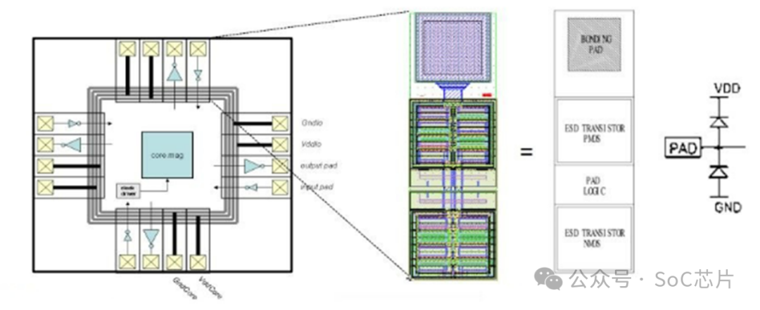
The I/O PAD is a critical part of the chip that connects to external circuits, typically consisting of bonding pads, circuits, power lines, and ground lines. The bonding pad (PAD) is used to connect the chip to the package substrate via gold wires, usually shaped as rectangles measuring several tens of micrometers. To avoid short circuits from the gold wires, a minimum distance must be maintained between PADs of different package types.
I/O PADs generally adopt a standard cell structure and have a set of I/O libraries, typically with equal height but varying widths. Sometimes, PAD refers to the entire I/O unit, while Bounding PAD refers specifically to the bonding pad.
1.1 Composition of Basic I/O Libraries
The I/O library typically includes the following types of PADs:
1. Power PADs: such as PAD_VDD, PAD_VSS, etc., responsible for powering the chip.
2. Signal PADs: including analog signal PADs (e.g., ANIN) and digital signal PADs (distinguishing between input and output). Analog signal PADs are usually a metal plate, and sometimes require users to add ESD protection circuits as needed.
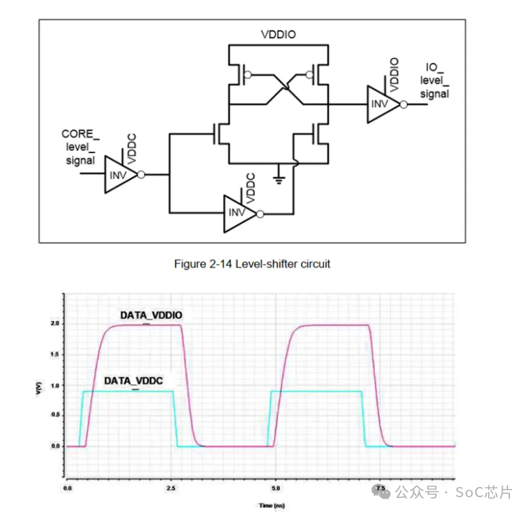
3. Voltage conversion circuits: achieve voltage conversion through level shifters, with voltage values depending on the chip process.
1.2 Circuit Design of I/O Units
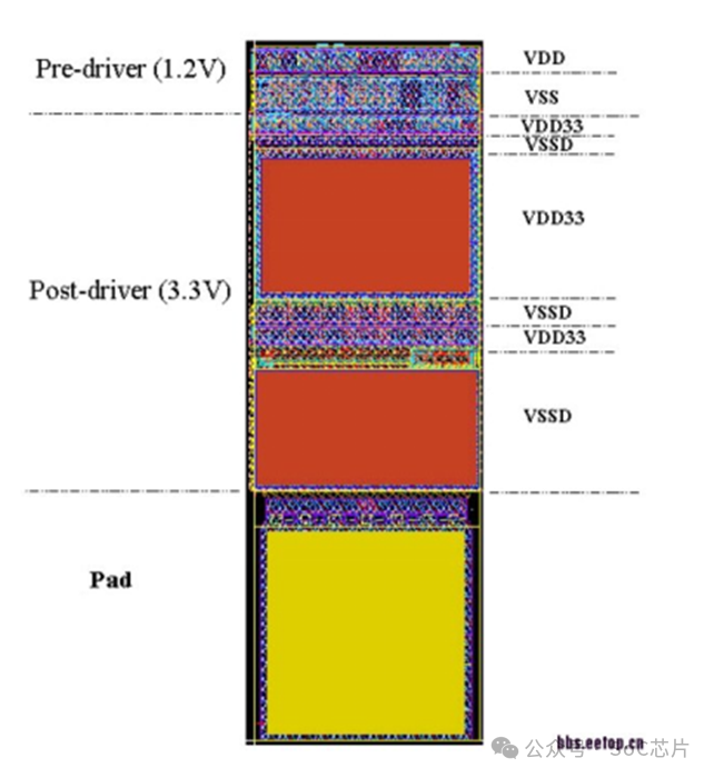
The main functions of the I/O unit circuit include ESD protection, voltage conversion (level shifter), Schmitt trigger, and power loop provision. The circuit can be further divided into pre-driver and post-driver, with the former responsible for the core voltage part, typically at a low voltage of 1.0V; the latter handles the high voltage part on the pad, usually at 3.3V, providing significant driving capability and ESD protection.

2. Common Types of Digital I/O Units
I/O units can be divided into input units, output units, and input/output units. Below are their specific designs and functions:
2.1 Input I/O Units
The input unit primarily protects the internal circuits, especially ESD protection. Its basic principle is to release static electricity through a low-impedance parallel channel and clamp the ESD voltage to a sufficiently low level to prevent damage to the chip.
Common ESD protection circuits include single diode + resistor structures and dual diode + resistor structures, used to discharge positive and negative high voltages, respectively.
2.2 Output I/O Units
The main function of the output unit is to provide driving capability while also having certain logic functions. Common output units include inverting output, non-inverting output, tri-state output, and metal mask programmed input/output units. High driving capability means faster charging speeds, requiring larger currents, thus MOSFETs with a large width-to-length ratio are more suitable for such applications.
For inverting output I/O PADs, an inverter chain is typically used to drive large capacitive loads. By reasonably designing the number of stages and driving capability of the inverter chain, the speed and performance of the entire circuit can be optimized.
2.3 Other I/O Units
• Non-inverting output I/O PAD: designed using “inversion + inversion” or even-numbered inverter chain designs.
• Tri-state output I/O PAD: used for bus control, presenting a high-impedance state when the bus is not in use.
• Open-drain output units: achieve line and function through pull-up networks, suitable for scenarios with multiple outputs in parallel.
2.4 Input/Output I/O Units
Input/output units typically switch their functions based on control signals. Depending on different connections, this unit can be configured for input or output mode, enabling flexible circuit design.
3. Other Basic Concepts of I/O PADs
3.1 Placement Methods of I/O PADs
The placement methods of I/O PADs include Inline and Staggered. When a single-layer inline pad ring cannot meet area requirements, staggered placement can be used to increase the number of PADs.
3.2 Pad Limited vs. Core Limited Design
Depending on the factors limiting chip size, designs can be classified as Pad Limited or Core Limited. For Pad Limited designs, staggered placement or flip chip packaging is typically used to accommodate more PADs.
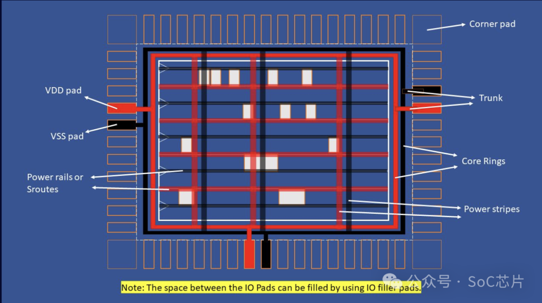
3.3 Corner PAD and Filler PAD
Corner PADs and Filler PADs are used to connect the corners of the chip and adjacent I/O PADs, forming power ground loops to ensure circuit continuity and reliability.
3.4 Selection of I/O PADs
When selecting I/O PADs, the number of Signal Pads and Power Pads should be determined based on specific application scenarios to ensure the stability and performance of the design.

Through a detailed discussion of the structure and design of chip I/O units, design engineers can better understand and apply I/O units, optimizing chip performance and ensuring reliability.