
In the field of optoelectronic hybrid computing power, many may be familiar with XiZhi Technology, founded by MIT PhD graduate Shen Yichen upon returning to China. Shen and his MIT classmate Nicholas Harris were co-authors of a paper, and they were both selected for the 2021 MIT Technology Review’s list of “35 Innovators Under 35”.
Similarly, based on this paper, Harris founded a company called Lightmatter in California. Recently, Lightmatter released a series of new products.

Image | Nicholas Harris (Source: https://www.linkedin.com/in/nicholas-harris-7114b233/)
The first new product released is a photonic super chip named Passage M1000 (hereafter referred to as “M1000”), which the company claims can achieve the world’s fastest AI interconnect. It utilizes groundbreaking 3D photonic interconnect layer technology, providing the highest bandwidth and largest chip complex for next-generation AI infrastructure silicon designs.
The second new product is a co-packaged optical device named Passage L200 (hereafter referred to as “L200”), which expands the overall chip area bandwidth through the world’s first edge-less I/O. The company states that this is the fastest co-packaged optical device in the AI field, employing a revolutionary 3D photonic interconnect solution that eliminates bandwidth bottlenecks, enabling an 8-fold increase in AI model training speed.
Lightmatter’s founder and CEO Nick Harris stated, “Bandwidth expansion has become a critical barrier to AI development. The engineering breakthroughs represented by the L200 series 3D co-packaged optical solutions provide foundational building blocks for next-generation AI processors and switches.”
Undoubtedly, Lightmatter aims to reshape the communication and computation of chips using photonic computing technology. The MIT website commented in a press release that this product accelerates the pace towards light-speed computing.

M1000: Capable of Supporting Interconnections for Thousands of GPUs in a Single Domain
The M1000 is a 3D photonic super chip designed for next-generation XPUs (X Processing Units) and switches, providing a total optical bandwidth of 114 Tbps for demanding AI infrastructure applications.
The benchmark platform for the M1000 exceeds 4000 square millimeters, serving as a multi-mask active photonic intermediary layer. This platform can construct the world’s largest 3D packaged bare chip complex, supporting interconnections for thousands of GPUs in a single domain.
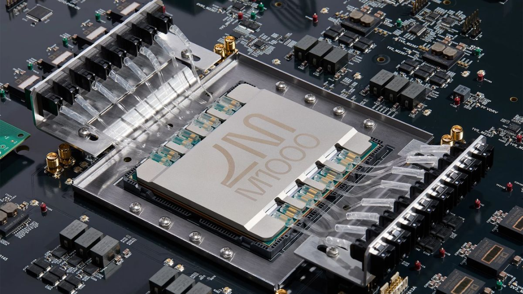
(Source: Lightmatter)
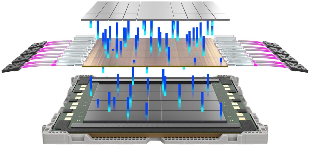
In existing chip designs, the interconnect bandwidth between processors, memory, and I/O small chips is relatively limited, as electrical I/O connections are confined to the edges of these chips. However, the M1000 can release electro-optical I/O at almost any location on its surface for stacked chip complexes, successfully overcoming the aforementioned limitations.
The M1000 achieves global intermediary layer interconnect through a large-scale reconfigurable waveguide network, capable of transmitting high-bandwidth wavelength division multiplexing (WDM) optical signals throughout the platform. It features fully integrated optical fiber interfaces, supporting a groundbreaking configuration of up to 256 optical fibers. Compared to traditional co-packaged optical devices (CPO) and similar solutions, the M1000 achieves an order of magnitude improvement in bandwidth performance within a smaller package size.
Currently, Lightmatter is closely collaborating with companies including GlobalFoundries and Amkor to achieve mass production of the M1000. It is reported that the M1000 utilizes GlobalFoundries’ Fotonix silicon photonics platform technology, which seamlessly integrates photonic components with high-performance CMOS logic into a single die, creating a mass production design that can scale with AI demands. The M1000 is expected to launch in the summer of 2025, along with the company’s light engine Guide.

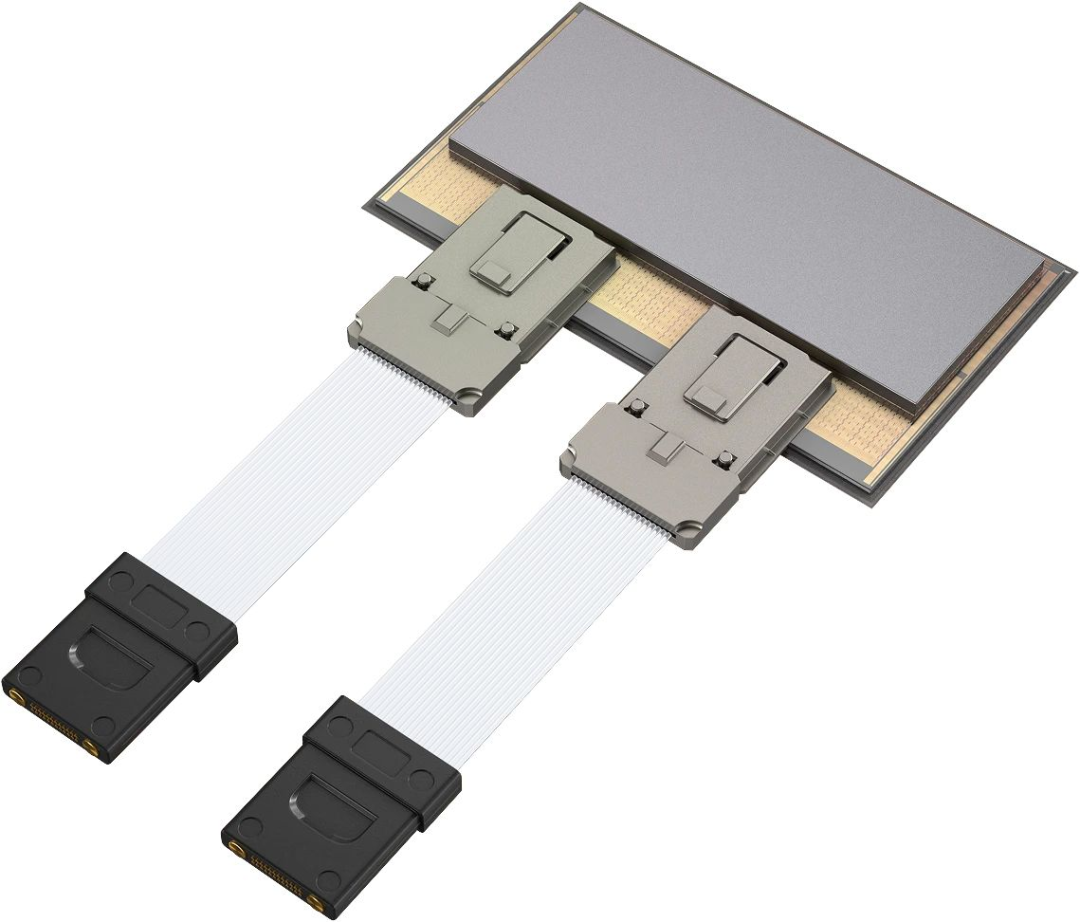
L200: The World’s First 3D Co-Packaged Optical Product
The second product launched, L200, is claimed by Lightmatter to be the world’s first 3D co-packaged optical product.
The L200 is designed to integrate with the latest XPU and switch chip designs, eliminating interconnect bandwidth bottlenecks to scale AI performance. The L200 3D co-packaged optical series includes two versions: 32 Tbps and 64 Tbps, achieving a performance increase of 5 to 10 times compared to existing solutions, allowing each chip package to exceed a total I/O bandwidth of 200 Tbps.
(Source: Lightmatter)
It is understood that current bandwidth expansion is far behind the improvements in computing performance. The continuous advancement of AI computing demands a fundamental transformation in interconnect technology. Current connection solutions, including electrical, optical, and traditional co-packaged optics, are limited by bandwidth, as their I/O interfaces are confined to the edges of the chips.
The L200 overcomes these limitations through the world’s first edge-less I/O, achieving bandwidth expansion across the entire chip area. This modular 3D co-packaged optical solution leverages general small chip interconnect technology for die-to-die (D2D) interfaces and facilitates seamless integration of scalable small chip architectures with next-generation XPUs and switches.
The L200 3D co-packaged optics integrate the latest small chip technology from Alphawave Semi, combining general small chip interconnect interfaces with optical communication-ready serializers/deserializers and Lightmatter’s photonic integrated circuit technology.
According to reports, Alphawave Semi’s advanced node electronic integrated circuits utilize standard wafer-on-chip technology and perform 3D integration on photonic integrated circuits. This 3D integration technology allows serializer/deserializer I/O to be placed anywhere on the chip, not just limited to its edges, providing each L200 with bandwidth equivalent to 40 pluggable optical transceivers. Additionally, multiple L200s can be integrated into a single package, making it widely applicable for XPU and switch applications.
The L200 features advanced redundancy and resilience designs, equipped with Lightmatter’s Guide light engine, with each module providing exceptional laser integration and total optical power to support the full bandwidth of the L200.
Currently, Lightmatter offers two product models: L200 (32 Tbps) and L200X (64 Tbps) 3D co-packaged optical engines. These solutions are based on Lightmatter’s proven Passage technology platform, with each waveguide/fiber providing 16 wavelength division multiplexing wavelengths and possessing state-of-the-art fully integrated photonic control capabilities.
It is understood that the L200 is specifically designed for mass production, with silicon photonics factories and outsourced packaging testing partners including GlobalFoundries, ASE, and Amkor.
Lightmatter’s L200 and L200X 3D co-packaged optical chips are expected to be launched in 2026, aiming to accelerate the time-to-market and performance enhancement of next-generation XPUs and switches required for next-generation foundational AI models.
(Source: Lightmatter)
Andrew Schmitt, founder and chief analyst of Cignal AI, commented: “AI data center interconnects face increasing bandwidth and power consumption challenges. Co-packaged optics—integrating optical devices directly into XPUs and switches—are the inevitable solution. Lightmatter’s bold approach provides the essential elements of co-packaged optics and offers a pathway for hyperscale data center operators and chip manufacturers to achieve high-performance systems.”

“The Timely Arrival of Photonic Chips”
Currently, humanity’s ability to integrate increasingly smaller transistors onto chips has facilitated the ubiquitous computing era we live in today. However, this approach is finally nearing its limits, with some experts claiming that Moore’s Law and the related Dennard Scaling are coming to an end. The timing of these technological bottlenecks is particularly unfortunate. In recent years, the demand for computing, especially AI, has grown exponentially, showing no signs of slowing down.
Meanwhile, for decades, there has been hope to develop optical chips that use photons instead of electrons for computational tasks. Optical chips offer the advantages of high speed and low energy consumption. However, getting them to function effectively has proven challenging.
In 2017, Harris and Shen Yichen, along with colleagues, co-authored the aforementioned Nature paper. In this paper, they utilized an optical chip scheme to compute the outputs of a neural network trained in the traditional manner.
In the paper, they introduced a “light path” composed of 56 programmable interferometer devices, which can decompose and reassemble light waves. This method solved the problem of correctly identifying vowels, successfully distinguishing three-quarters of the vowels in 180 cases.
Although this result temporarily fell short of the over 90% accuracy rate of conventional computers, the circuit’s performance was still impressive. Shortly thereafter, Harris and Shen Yichen each founded their own startups in the US and China, respectively.
Once such neural networks can function and be trained on optical chips, certain inference processes, such as identifying the sounds corresponding to vowels, will flow as smoothly as photons through the chip, while also being fast and energy-efficient.
Before entering MIT for his PhD, Harris worked at semiconductor company Micron Technology, researching the fundamental devices behind integrated chips. This experience made him realize that the traditional method of improving computer performance by cramming more transistors onto each chip had reached its limits.
At that time, he saw the roadmap for the computing field slowing down and sought to understand how to continue advancing it. So, what methods could enhance computer performance? Quantum computing and photonics were two of those pathways.
Harris came to MIT to pursue a PhD under the guidance of Dirk Englund, an associate professor in the Department of Electrical Engineering and Computer Science, studying photonic quantum computing. As part of his doctoral work, he built silicon-based integrated photonic chips capable of using light instead of electricity to send and process information.
This work led to dozens of patent applications and over 80 research papers published in prestigious journals such as Nature. However, at MIT, another technology also caught Harris’s attention.
“I remember walking down the hall and seeing students pouring out of these auditorium-sized classrooms to watch live-streamed lecture videos, listening to professors talk about deep learning,” Harris told the media. “Everyone on campus knew that deep learning was going to be a big deal, so I started to learn more about it, and we realized that the system I was building for photonic quantum computing could actually be used for deep learning.”
Harris originally planned to become a professor after obtaining his PhD, but he realized that entrepreneurship could attract more funding and accelerate innovation. Thus, he teamed up with Darius Bunandar (a 2019 MIT PhD graduate) and Thomas Graham (a 2018 MIT MBA graduate), both of whom studied in Englund’s lab. The three co-founders successfully entered the startup field by winning the $100,000 MIT Startup Competition in 2017.

Rethinking the Lifeline of Chips
At Lightmatter, Harris aims to sustain significant advancements in computing by rethinking the lifeline of chips. The company relies not only on electricity but also on light for data processing and transmission. Its first two products are a chip specifically designed for AI computations and an interconnect that facilitates data transfer between chips, both utilizing photons and electrons to drive more efficient computations.
Harris is currently addressing two questions: How do chips communicate? How do AI computations occur? Lightmatter’s previous two products, Envise and Passage, are capable of solving both of these issues simultaneously.
Given the severity of the issues and the demand for AI, Lightmatter raised nearly $300 million in funding in 2023, achieving a valuation of $1.2 billion. Harris told the media, “We will build a platform on interconnect technology composed of hundreds of thousands of next-generation computing units. Without the technology we are developing, this would be impossible.”
It is understood that Lightmatter’s previous generation product, the Envise chip, achieved the computing aspects that electronics excel at, such as storage functions, while also combining them with aspects where light excels, such as performing large-scale matrix multiplication in deep learning models.
Utilizing photonics allows for multiple computations to be executed simultaneously, as data is input in the form of different colors of light. One color of light might represent a photo of a dog, another color might represent a photo of a cat, and yet another color might represent a tree. By executing all three operations simultaneously through the same optical computing unit, i.e., allowing this matrix accelerator to perform all three operations, the computational capacity per unit area can be increased, and existing hardware can be reused, thereby improving energy efficiency.
Optical channels leverage the advantages of light’s delay and bandwidth to connect processors in a manner similar to how fiber optic cables transmit data over long distances. It also enables a chip the size of an entire wafer to operate as a single processor. Transmitting information between chips is crucial for running large-scale server farms that support cloud computing and AI models like ChatGPT.
It is predicted that by 2040, approximately 80% of global energy usage will be dedicated to data centers and computing, with AI accounting for a significant portion of that. When we examine the training computation deployments of these large AI models, we find that they will consume hundreds of megawatts of electricity, reaching the scale of entire cities.
Lightmatter is currently collaborating with chip manufacturers and cloud service providers to achieve large-scale deployment. Harris pointed out that since the company’s devices operate on silicon wafers, they can be produced using existing semiconductor manufacturing facilities without requiring large-scale changes to the processes.
In the future, the company will continue to explore all components of computing to identify where light can accelerate them, making them more energy-efficient and faster. Ultimately, Lightmatter aims to contribute to building the next generation of computers, all centered around light.
References:
https://www.linkedin.com/in/nicholas-harris-7114b233/
https://mp.weixin.qq.com/s/pcytbDIzrEJ3T9s69afMZg
https://lightmatter.co/
Operations/Layout: He Chenlong


 01/ US Biological Database Bans Chinese Users, Industry Insiders: China Has Long Had Countermeasures02/ DeepMind Predicts AGI May Arrive by 2030, Identifies Four Methods to Reduce AI Errors, Proposes Two Defenses Against Misalignment Issues03/ Scientists Design 3D Force Self-Decoupling Haptic Sensors, Simplifying Data Collection Processes, Usable for Measuring Robot Force Distribution04/ Fudan Team Develops Domestic “Unlimited” Chip by Bypassing Silicon-Based Materials, Breaking Through Engineering Bottlenecks in Two-Dimensional Semiconductor Electronics05/ Harvard Team Creates AI-Driven Molecular-Level “Microscope”, Providing Powerful New Tools for Researching DNA Regulatory Elements, Capable of Observing Gene Regulation Processes with Higher Precision