In the modern world, no one can say they are unrelated to “semiconductors.” Semiconductors sound rigid and cold, but they are not just a concern for engineers in scientific parks; the smartphones you swipe, the computers you use, the televisions you watch, and the speakers you listen to all contain semiconductor components. It can be said that without semiconductors, there would be no lightweight and user-friendly high-tech products in the modern world.
The importance of semiconductors is self-evident, even being hailed as the fourth most important invention in the world. The Atlantic Monthly once enlisted scientists, historians, and technology experts to rank major inventions in human history, with semiconductors coming in fourth, preceded only by the printing press, electricity, and penicillin.
When it comes to semiconductors, one must mention the foundation of semiconductors—the materials.
In the modern science of the twentieth century, especially with the development of quantum mechanics, it was understood that metallic materials have good electrical and thermal conductivity, while ceramic materials do not. Prior to the emergence of these properties, people’s understanding of surrounding objects was still relatively macroscopic. Between these two is semiconductor material.


British scientist Faraday (Michael Faraday, 1791~1867) made many contributions to electromagnetism, but perhaps less known is his discovery in 1833 of a semiconductor material: silver sulfide, because its resistance decreases with increasing temperature. At the time, this was considered somewhat peculiar but did not spark much excitement.
However, today we know that as the temperature rises, lattice vibrations intensify, causing resistance to increase, but for semiconductors, increasing temperature actually increases the concentration of free carriers, aiding conductivity.
This was the first discovery of the semiconductor phenomenon.
Shortly thereafter, in 1839, French scientist Becquerel discovered that a junction formed by a semiconductor and an electrolyte generates a voltage when illuminated, which is the well-known photovoltaic effect recognized later as the second characteristic of semiconductors.
In 1874, German scientist Braun (Ferdinand Braun, 1850~1918) observed that the conductivity of certain sulfides is related to the direction of the applied electric field, meaning it has directional conductivity; applying a positive voltage across its terminals allows it to conduct; reversing the voltage polarity prevents conduction. This is the rectification effect unique to semiconductors, marking the third characteristic. That same year, Schuster discovered the rectification effect of copper and copper oxide.
In 1873, British scientist Smith discovered the photoconductivity effect of selenium crystals, where conductivity increases under illumination, marking another unique property of semiconductors.
Although these four effects of semiconductors were discovered before 1880, the term “semiconductor” was likely first used by Conybeare and Weiss in 1911. The summarization of these four characteristics of semiconductors was not completed until December 1947 by Bell Labs.
It wasn’t until 1906 that American electrical inventor Pickard (G. W. Pickard, 1877~1956) invented the first solid-state electronic component: the radio wave detector (cat’s whisker), using the rectifying function produced by the contact of metal with silicon or lead sulfide to detect radio waves.
In terms of rectification theory, German scientist Schottky (Walter Schottky, 1886~1976) published an important paper on rectification theory in 1939 in the German Physical Society, making many inferences. He believed that there is a potential barrier between metals and semiconductors, and his main contribution was accurately calculating the shape and width of this potential barrier.
The rectification theory accepted today was developed in 1942 by Sommerfeld’s student Bethe, who proposed the thermionic emission theory, suggesting that high-energy electrons can overcome the potential barrier to reach the other side, aligning well with experimental results.
In the field of semiconductors, the band theory is equally important as the rectification theory. Bloch (Felix Bloch, 1905~1983) made significant contributions in this area, with his theorem adding periodic terms to the electron wave function, opening the way for band theory. On the other hand, German scientist Peierls pointed out in 1929 that an almost completely filled energy band can be explained by some positively charged carriers, marking the origin of the concept of holes; he later proposed perturbation theory to explain the existence of energy gaps.

In the early 20th century, although people’s understanding of semiconductors was limited, research on the application of semiconductor materials was quite active.
In the 1920s, the development of solid-state physics and quantum mechanics, along with the continuous improvement of band theory, led to a deeper understanding of the electronic states and transport processes in semiconductor materials, as well as a more profound understanding of the structural properties, impurities, and defects in semiconductor materials, improving the integrity and purity of semiconductor crystals.
In the 1950s, to improve transistor characteristics and enhance their stability, the preparation technology of semiconductor materials developed rapidly. Although silicon achieved great success in microelectronics technology, its progress in silicon-based light-emitting devices was slow due to the constraints of indirect band gaps.
With the proposal of the concept of semiconductor superlattices and the advancement of advanced epitaxial growth technologies such as molecular beam epitaxy, metal-organic chemical vapor deposition, and chemical beam epitaxy, a series of crystalline, amorphous thin films, and ultra-thin microstructural materials were successfully grown. This not only advanced semiconductor physics and the design and manufacture of semiconductor devices from the past so-called “impurity engineering” to “band engineering,” laying the foundation for a new generation of devices based on quantum effects.
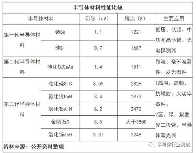

The first generation of semiconductors is “element semiconductors,” typically silicon-based and germanium-based semiconductors. Among these, silicon-based semiconductor technology is more mature and widely used, often replacing the term element semiconductors with silicon-based semiconductors. In fact, currently, over 95% of semiconductor chips and devices globally are produced using silicon wafers as the foundational functional material.
Represented by silicon materials, the first generation of semiconductor materials replaced bulky vacuum tubes, leading to the development of the microelectronics industry centered around integrated circuits and a leap in the entire IT industry, widely used in information processing and automatic control fields.
However, in the 1950s, germanium dominated the semiconductor field, mainly used in low-voltage, low-frequency, medium-power transistors and photodetectors. However, germanium-based semiconductor devices had poor high-temperature and radiation resistance, gradually being replaced by silicon-based devices by the late 1960s. Semiconductor devices made from silicon exhibit better high-temperature and radiation resistance.
In 1960, a 0.75-inch (about 20mm) single crystal silicon wafer appeared.
In 1965, discrete transistor devices began using small silicon wafers of 1.25 inches. Afterward, developments progressed to 2-inch, 3-inch, and by 1975, 4-inch single crystal silicon wafers began to be popular in the global market, followed by 5-inch, 6-inch, and 8-inch wafers. In 2001, 12-inch silicon wafers were put into use, and it is expected that by 2020, 18-inch (450mm) silicon wafers will begin to be used.
It is understood that silicon wafers account for about 32% of the entire semiconductor materials market, with an industry market space of about $7.6 billion. The domestic semiconductor silicon wafer market size is around 13 billion RMB, accounting for 42.5% of the total domestic semiconductor manufacturing materials.
This field is mainly monopolized by Japanese manufacturers. The domestic 6-inch silicon wafer localization rate is 50%, the 8-inch silicon wafer localization rate is 10%, and the 12-inch silicon wafer is completely reliant on imports.
Currently, the silicon wafers in use are 200mm (8 inches) and 300mm (12 inches). As the wafer area increases, more integrated circuits (ICs) can be produced on the same wafer, lowering costs; thus, the trend in silicon wafer development is towards larger sizes. 12-inch silicon wafers are primarily used to produce memory, digital circuit chips, and mixed-signal circuit chips with feature sizes of 90nm-28nm and below (16nm and 14nm), which is the mainstream for wafer factories’ expansion.
Due to dual pressures of funding and technology, the pace of wafer factories transitioning to 450mm (18-inch) production lines has slowed. According to international predictions, it may be around 2020 before the development technology for 450mm silicon wafers achieves initial mass production.

Since the 1990s, with the rapid development of mobile communications and the rise of information superhighways based on fiber optic communications and the internet, second-generation semiconductor materials represented by gallium arsenide (GaAs) and indium phosphide (InP) have begun to emerge.
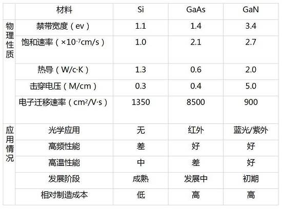
The second generation of semiconductor materials is compound semiconductors. Compound semiconductors are represented by gallium arsenide (GaAs), indium phosphide (InP), and gallium nitride (GaN), including many other III-V group compound semiconductors. Among these compounds, the most used in commercial semiconductor devices are gallium arsenide (GaAs) and gallium phosphide (GaAsP), indium phosphide (InP), gallium aluminum arsenide (GaAlAs), and indium gallium phosphide (InGaP). Among them, gallium arsenide technology is more mature and widely applied.
Materials such as GaAs and InP are suitable for making high-speed, high-frequency, high-power, and optoelectronic devices. They are excellent materials for producing high-performance microwave, millimeter-wave devices, and light-emitting devices, widely used in satellite communications, mobile communications, optical communications, GPS navigation, and other fields. However, GaAs and InP materials are scarce, expensive, and toxic, potentially polluting the environment. InP is even considered a suspected carcinogen, limiting the application of second-generation semiconductor materials significantly.
However, the properties of compound semiconductors differ from silicon semiconductors in two main ways:
First, compound semiconductors have a much higher electron mobility than silicon semiconductors, making them suitable for high-frequency transmission. They are used in radio communications such as mobile phones, base stations, wireless local area networks, satellite communications, and satellite positioning.
Second, compound semiconductors have a direct bandgap, unlike silicon semiconductors, making them suitable for light-emitting applications such as light-emitting diodes (LEDs), laser diodes (LDs), photodetectors (PIN), and solar cells. They can be used to manufacture ultra-high-speed integrated circuits, microwave devices, lasers, optoelectronic devices, as well as radiation-resistant and high-temperature devices, which are of great significance for national defense, aerospace, and high-tech research.
Currently, the five largest global GaAs semiconductor manufacturers are Skyworks, Triquint, RFMD, Avago, and Winbond, accounting for about 65% of the global total. In the GaAs raw materials sector, IQE, Qorvo, and Kopin occupy 67.3% of the market share.

In recent years, third-generation semiconductor materials have become the focus of competition in the global semiconductor market due to their superior performance and enormous market prospects.
The so-called third-generation semiconductor materials mainly include SiC, GaN, and diamond, and are also known as wide bandgap semiconductor materials because their bandgap (Eg) is greater than or equal to 2.3 electron volts (eV).
Currently, the operating conditions for electronic devices are becoming increasingly harsh, requiring adaptation to high-frequency, high-power, high-temperature, and radiation-resistant environments. To meet the future demands for electronic devices, new materials must be adopted to maximize the intrinsic performance of electronic components.
Compared to the first and second generation of semiconductor materials, third-generation semiconductor materials have advantages such as high thermal conductivity, high breakdown field strength, high saturation electron drift velocity, and high bonding energy, meeting modern electronic technology’s new requirements for high temperature, high power, high voltage, high frequency, and radiation resistance. They are promising materials in the field of semiconductor materials.
They have significant application prospects in national defense, aerospace, oil exploration, optical storage, and other fields, potentially reducing energy losses by more than 50% in many strategic industries such as broadband communications, solar energy, automotive manufacturing, semiconductor lighting, and smart grids, which could reduce equipment size by over 75%, marking a milestone in the development of human technology.
Currently, devices made from these materials can operate at temperatures exceeding 600 °C and withstand radiation of 1×10⁶ rad; small gate-width GaN HEMT devices achieve power densities of 40 W/mm at 4 GHz, 30 W/mm at 8 GHz, 9.1 W/mm at 18 GHz, 10.5 W/mm at 40 GHz, and 2.1 W/mm at 80.5 GHz. Therefore, wide bandgap semiconductor technology has become a new driving force in today’s electronics industry.
From the current research situation of wide bandgap semiconductor materials and devices, the focus is mostly on silicon carbide (SiC) and gallium nitride (GaN) technologies, with SiC technology being the most mature and progressing rapidly. GaN technology is widely applied, especially in optoelectronic device applications. Research on wide bandgap semiconductor technologies such as aluminum nitride, diamond, and zinc oxide is relatively limited, but given their material advantages, they hold great development potential, and as research continues, their application prospects are expected to be very broad.

Among the existing wide bandgap semiconductor materials, silicon carbide materials are the most mature in research.
Compared to silicon, silicon carbide has many advantages: it has 10 times the electric field strength, 3 times the thermal conductivity, 3 times the bandgap width, and 1 time the saturation drift velocity. Because of these characteristics, devices made from silicon carbide can be used in extreme environmental conditions. Microwave, high-frequency, and short-wavelength devices are currently mature application markets. A 42GHz frequency SiC MESFET is used in military phased array radar and communication broadcast systems, while high-brightness blue LEDs using silicon carbide as a substrate are key components in full-color large-area displays.
In application fields, silicon carbide has the following advantages:
1. SiC materials applied in high-speed rail can save more than 20% of energy and reduce the size of power systems;
2. SiC materials applied in new energy vehicles can reduce energy consumption by 20%;
3. SiC materials applied in home appliances can save 50% of energy;
4. SiC materials applied in wind power generation can improve efficiency by 20%;
5. SiC materials applied in solar energy can reduce photovoltaic conversion losses by more than 25%;
6. SiC materials applied in industrial motors can save 30%-50% of energy;
7. SiC materials applied in ultra-high voltage direct current transmission and smart grid can reduce power loss by 60%, while improving power supply efficiency by more than 40%;
8. SiC materials applied in big data can significantly reduce energy consumption in data centers;
9. SiC materials applied in communications can significantly improve signal transmission efficiency and transmission security and stability;
10. SiC materials applied in aerospace can reduce equipment loss by 30%-50%, triple the operating frequency, reduce the volume of inductors and capacitors by three times, and significantly reduce the weight of heat sinks.
Silicon carbide devices and circuits possess super strong performance and broad application prospects, thus receiving significant attention in the industry, essentially forming a tripartite situation among the United States, Europe, and Japan. Currently, the main companies commercializing silicon carbide single crystal polished wafers internationally include Cree, Bandgap, Dow Corning, II-VI, and Intrinsic in the United States; Nippon and Sixon in Japan; Okmetic in Finland; and SiCrystal in Germany, among others.

Gallium nitride (GaN) is a III-V compound semiconductor material synthesized by Jonason et al. in 1928.
Gallium nitride is a compound of nitrogen and gallium, with a structure similar to zinc blende and high hardness. As an emerging semiconductor processing technology, it offers multiple advantages over silicon. Compared to silicon devices, GaN has made leaps in power conversion efficiency and power density.
Compared to silicon, gallium arsenide, germanium, and even silicon carbide devices, GaN devices can operate under higher frequencies, higher power, and higher temperatures. Additionally, gallium nitride devices can be applied in the high-frequency band ranging from 1 to 110GHz, covering mobile communications, wireless networks, point-to-point, and point-to-multipoint microwave communications, and radar applications. In recent years, III-nitride materials represented by GaN have received widespread attention due to their application prospects in optoelectronics and microwave devices.
As a semiconductor material with unique optoelectronic properties, GaN applications can be divided into two parts:
By leveraging GaN semiconductor materials’ excellent performance under high temperature, high frequency, and high power working conditions, they can replace some silicon and other compound semiconductor materials;
By utilizing GaN semiconductor materials’ wide bandgap and unique properties for exciting blue light to develop new optoelectronic application products.
Currently, GaN optoelectronic devices and electronic devices have distinct competitive advantages in optical storage, laser printing, high-brightness LEDs, and wireless base stations, with high-brightness LEDs, blue laser diodes, and power transistors being the most interesting and focused areas in current device manufacturing.
Currently, the entire GaN power semiconductor industry is in its infancy, with various countries’ policies vigorously promoting the development of this industry. Major international semiconductor companies are also turning their attention to the GaN power semiconductor sector, with ongoing acquisitions and collaborations among GaN device manufacturers.

Semiconductor wafer manufacturing materials are closely linked to wafer manufacturing capacity. In recent years, with the growth in shipment numbers, semiconductor manufacturing materials revenue has grown from $23 billion in 2013 to $24.2 billion in 2016, with a compound annual growth rate of about 1.8%. From the details, it can be seen that the sales share of silicon wafers decreased from 35% in 2013 to 30% in 2016.
From the 2016 wafer manufacturing materials classification share, silicon wafers accounted for the largest share at 30%. As downstream smart terminal machines’ requirements for chip performance continue to rise, so do the quality requirements for silicon wafers. Coupled with the driving forces of Moore’s Law and cost factors, silicon wafers are steadily developing towards larger sizes. Currently, the mainstream silicon wafer sizes globally are concentrated at 300mm and 200mm, with shipment shares of 70% and 20%, respectively.
According to the 2016 revenue data of major global silicon wafer manufacturers, the top six manufacturers hold over 90% of the global market share, with the top two Japanese manufacturers, Shin-Etsu and SUMCO, together accounting for over 50% of the global market share. Taiwan’s GlobalWafers, due to the acquisition of Singapore’s SunEdison Semiconductor, is currently ranked third globally, with a sales share of 17% in 2016.
The market conditions for semiconductor materials in China are similar to those globally, with silicon wafers and packaging substrates being the two largest categories of materials in wafer manufacturing and packaging materials. From the growth trend chart, it can be seen that the Chinese semiconductor materials market grew rapidly from 2016 to 2017, with growth rates exceeding 10% for both wafer manufacturing materials and packaging materials.
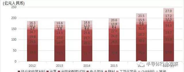 Changes in China’s wafer manufacturing materials market from 2012 to 2017

Research on SiC and GaN materials and devices in China started relatively late, and the level is lower compared to foreign countries. The progress of domestic third-generation semiconductor research is hindered by original innovation issues. Most research institutes and related production enterprises in the new materials field in China are short-sighted, unable to tolerate the long-term situation of “only investing without output.” Therefore, original innovation in new materials, represented by third-generation semiconductor materials, is difficult to achieve.
However, with increasing support from the national strategic level, especially given China’s strong industrial foundation in energy conservation and emission reduction, and the urgent market demand, China is expected to concentrate its advantageous forces to achieve a technological breakthrough!
Source: Semiconductor Industry Observation
Editor: Milk Cap Four Seasons Green