●IIC Bus
1. Concept of IIC
I²C stands for Inter-Integrated Circuit, using two bidirectional lines: one Serial Data Line (SDA) and one Serial Clock (SCL). SCL: The rising edge inputs data into each EEPROM device; the falling edge drives the EEPROM device to output data (edge-triggered). SDA: The bidirectional data line is an open-drain configuration, in a “wired AND” relationship with any number of other open-drain and open-collector devices.
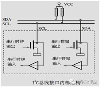 The internal circuit structure of the SDA and SCL pins of each I2C device is the same. The output driver is connected to the input buffer. The output is an open-drain field-effect transistor, and the input buffer is a high-impedance non-inverting amplifier. This circuit has two characteristics:
1) Since SDA and SCL are open-drain structures (OD), they must be connected to pull-up resistors, with typical values of 1.8k, 4.7k, and 10k, but 1.8k provides the best performance; when the bus is idle, both lines are high. Any device connected to the bus that outputs a low level will pull the bus signal low, meaning that the SDA and SCL of each device are in a “wired AND” relationship.
2) The pins detect the level of the output signal while outputting, checking whether it matches the previously output level, providing a hardware basis for “clock synchronization” and “bus arbitration”.
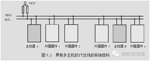
2. IIC Master-Slave Devices
All peripheral devices in the system have a 7-bit “slave device address code”, where the high 4 bits are the device type determined by the manufacturer, and the low 3 bits are the device pin definition address defined by the user. The master device establishes a multi-device communication mechanism through the address code, thereby eliminating the need for chip select lines for peripheral devices on the I2C bus. Thus, regardless of how many devices are connected to the bus, the system remains a simple two-wire structure. Devices connected to the bus are classified as master and slave; the master must be a logic module with a CPU. Only one master can be enabled on the same bus at the same time, but there can be multiple slaves. The number of slaves is limited by the address space and the maximum bus capacitance of 400pF. Both can transmit data, but the slave device cannot initiate a transmission, and the transmission is controlled by the master device.
3. Speed
Standard mode: 100kHz;
Fast mode: 400kHz;
High-speed mode: 3.4MHz;
There is no need to use high-speed SCL; keep SCL at 100k or below and forget about it…
4. Protocol
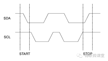
1) Idle State
The I2C bus is in an idle state when both SDA and SCL signal lines are at a high level. At this time, the output stage field-effect transistors of all devices are in the cutoff state, releasing the bus, and both signal lines are pulled high by their respective pull-up resistors.
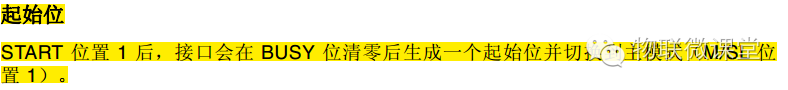
2) Start Signal
When SCL is high, SDA transitions from high to low; the start signal is a level transition timing signal, not a level signal.
3) Stop Signal
When SCL is high, SDA transitions from low to high; the stop signal is also a level transition timing signal, not a level signal.
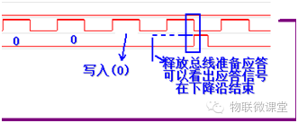
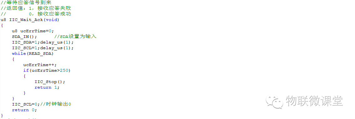
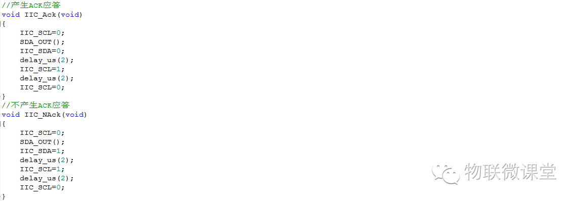
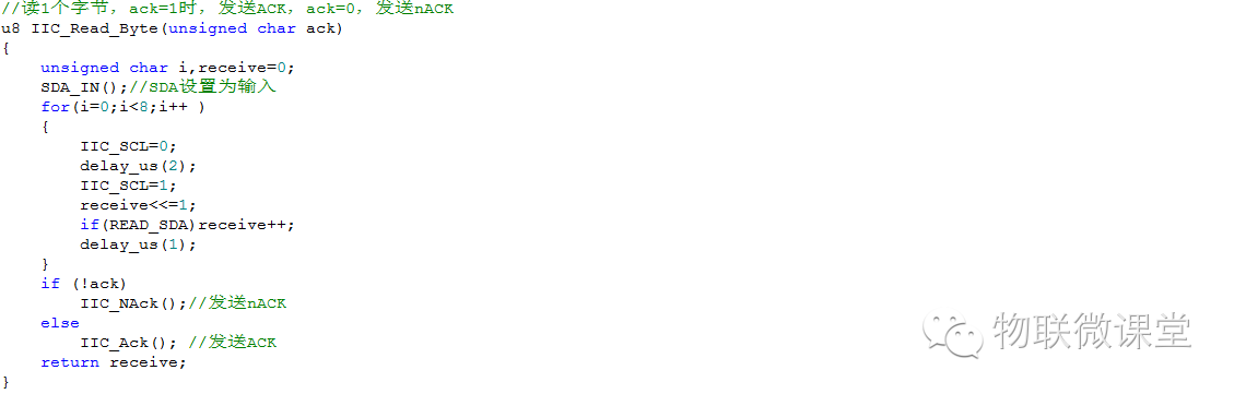
 4) Acknowledge Signal
After sending each byte, the transmitter releases the data line during the 9th clock pulse, and the receiver responds with an acknowledge signal. A low-level acknowledge signal is defined as a valid acknowledge bit (ACK), indicating that the receiver has successfully received the byte; a high-level signal is defined as a non-acknowledge bit (NACK), generally indicating that the receiver did not successfully receive the byte. The requirement for the valid acknowledge bit (ACK) is that the receiver pulls the SDA line low during the low period before the 9th clock pulse and ensures that it remains a stable low during the high period of that clock. If the receiver is the master, it sends a NACK signal after receiving the last byte to notify the slave transmitter to end data transmission and release the SDA line for the master receiver to send a stop signal P.
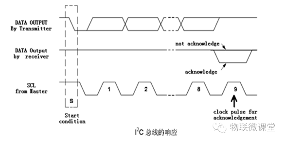
The following is the sampling result from a logic analyzer: after releasing the bus, if there is no acknowledge signal, SDA should remain high, but as shown in the blue dashed line part of the figure, it is pulled low, indicating that an acknowledge signal was received. The two pieces of information provided here are: 1) The receiver pulls SDA low during the low period before the rising edge of SCL; 2) The acknowledge signal remains until the falling edge of SCL ends, as indicated by the red markings earlier.
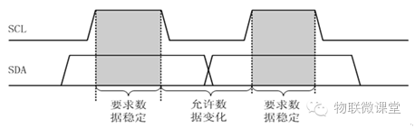
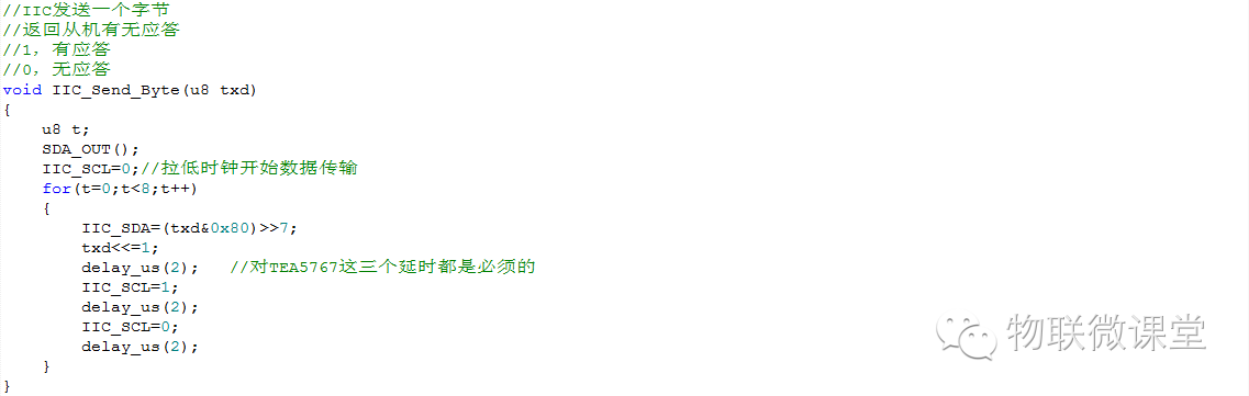
 5) Data Validity
When transmitting data on the I2C bus, the data on the data line must remain stable during the high period of the clock signal; changes to the high or low state of the data line are only allowed during the low period of the clock line. My understanding: although it only requires stability during the high level, there should be a lead time, meaning that data must be ready before the rising edge of SCL, because as pointed out in the previous article on the I2C bus (Part 1) – Overview, data is input into the device (EEPROM) at the rising edge of SCL.
4. Arbitration and Synchronization
1) Clock Synchronization All masters generate their own clocks on the SCL line to transmit messages on the I2C bus; data is only valid during the high period of the clock. Therefore, a definite clock is needed for bitwise arbitration. Since all SCL lines are connected together, as long as one is low, SCL will be pulled low. When a certain master pulls SCL low, if other masters find that their SCL is different from the bus, they will enter a high-level waiting state. 2) Arbitration Arbitration occurs on the SDA line, similar to clock synchronization; when one master pulls SDA low, SDA will go low. If another master finds that its SDA is different from the bus, it will exit the competition.
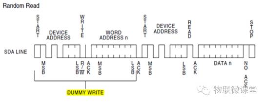
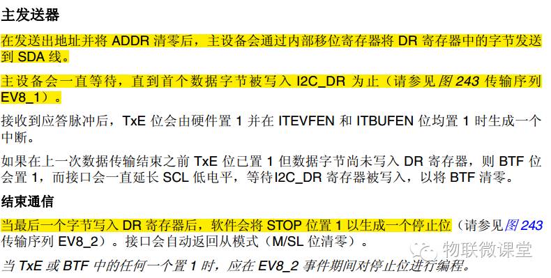
5. Data Transmission
Master Device Sending
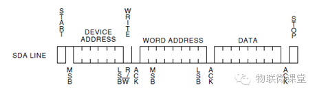
During data transmission, the first step is to send a 7-bit slave address, followed by the 8th bit which indicates data direction R/W, where 0 means send (write) and 1 means request data (read). In fact, this process sends one byte, with the high 4 bits determined by the IC manufacturer and the last 3 bits defined by the user (for example, some EEPROMs have A0, A1, A2 pins, thus allowing user-defined addresses). The last bit is the read/write signal. 1) Send start bit. 2) Send the slave device address and read/write selection bit; release the bus and wait for the EEPROM to pull the bus low to acknowledge; if the EEPROM successfully receives it, it will acknowledge; if there is no successful handshake or the data sent is incorrect, the EEPROM will not acknowledge, requiring a resend or termination. 3) Send the internal register address you want to write to; the EEPROM acknowledges it. 4) Send data. 5) Send stop bit.
Master Device Receiving Data
1) Send start bit; 2) Send slave address + 0; 3) Send internal register address; 4) Resend start bit; 5) Resend slave address + 1; 6) Read data. 7) The master receiver does not send an ACK signal after receiving the last byte. Thus, the slave transmitter releases the SDA line to allow the master to send a P signal to end transmission. 8) Send stop bit.
● STM32 IIC Interface 1. IIC Function Description


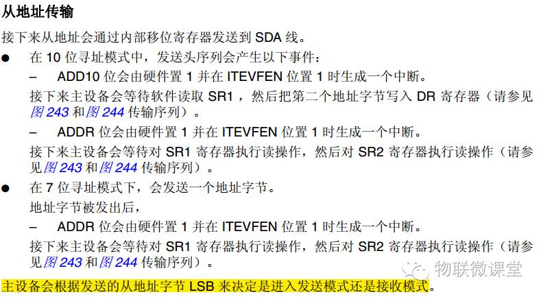
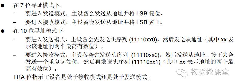
2. Register Description
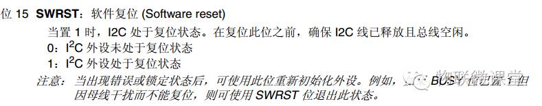
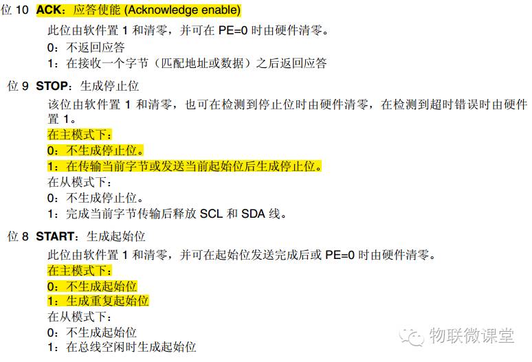
1) Control Register I2C_CR1
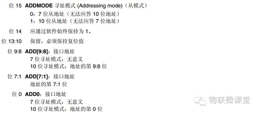
2) I2C Own Address Register I2C_OAR1
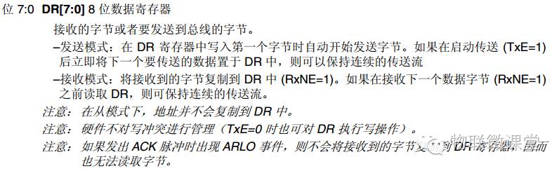
3) I2C Data Register
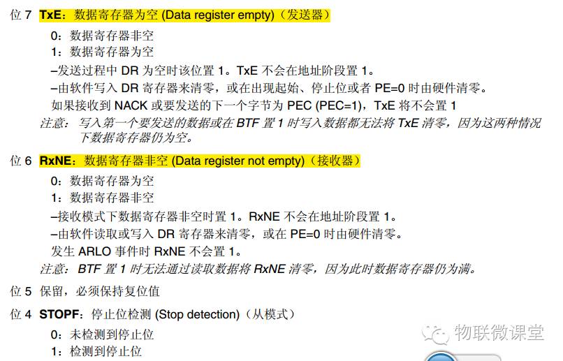
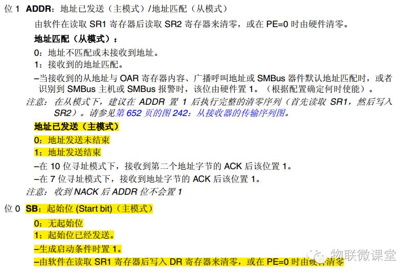
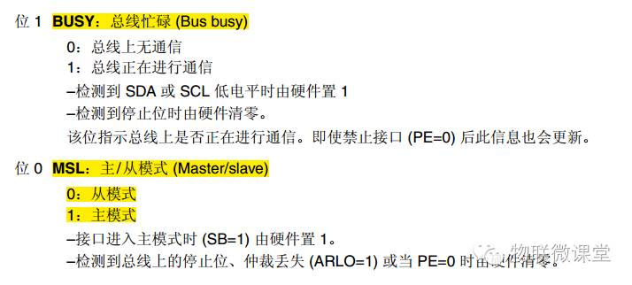
 4) I2C Status Register I2C_SR1
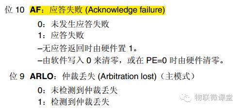
 4) I2C Status Register I2C_SR2
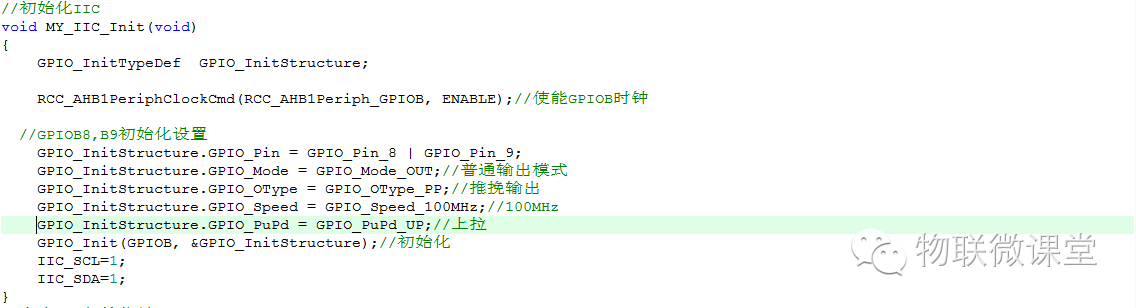
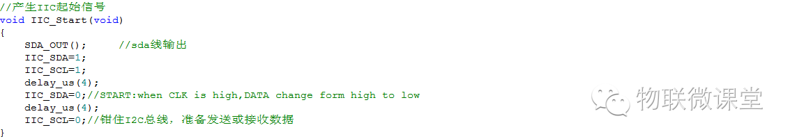
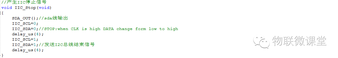
● Code
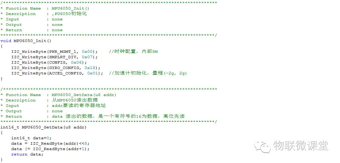
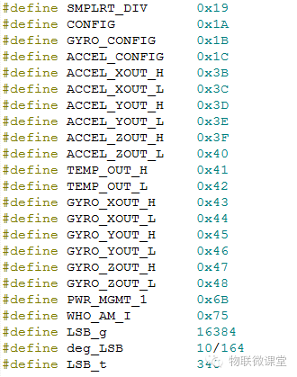
● Slave Device MPU6050
1. Function Introduction
The MPU-60X0 is a nine-axis motion sensor that integrates a 3-axis gyroscope, a 3-axis accelerometer, and an expandable digital motion processor. It can connect to a third-party digital sensor using the I2C bus, and after expansion, it can output 9-axis data via I2C or SPI interface (the SPI bus can only be used with MPU6000). The measurement range of the sensor can be controlled by the user; the gyroscope range can be (-250, 250), (-500, 500), (-1000, 1000), (-2000, 2000) (degrees/s), and the accelerometer range can be (-2, 2), (-4, 4), (-8, 8), (-16, 16) (in g). The communication speed is up to 400kHz in I2C mode. Pin: Pin 23 is the I2C serial clock, Pin 24 is the I2C data, and Pin 9 is the slave address line; the MPU6050 slave device address is 110100x, where the x bit is determined by Pin 9, so there can only be 2 motion sensors on one I2C bus. It has a built-in temperature sensor and provides an 8M clock internally.
2. Commands
The process of using IIC to operate the MPU6050 is the process of sending commands and receiving data.
 3. Initialization and Data Transmission