(Source: design-reuse)
Recently, the American semiconductor startup Zero ASIC announced the launch of the world’s first open standard eFPGA IP product, Platypus. According to them, Platypus is the first and only commercial eFPGA IP product with the following features: a 100% open and standardized FPGA architecture, a 100% open-source FPGA bitstream format, and 100% open-source FPGA development tools.
Data shows that Zero ASIC is a semiconductor startup based in Cambridge, Massachusetts. The company’s mission is to democratize silicon through chips and automation. Zero ASIC is building the world’s first composable chip platform, enabling billions of unique silicon systems to be assembled from a ready-made chip catalog in just hours.
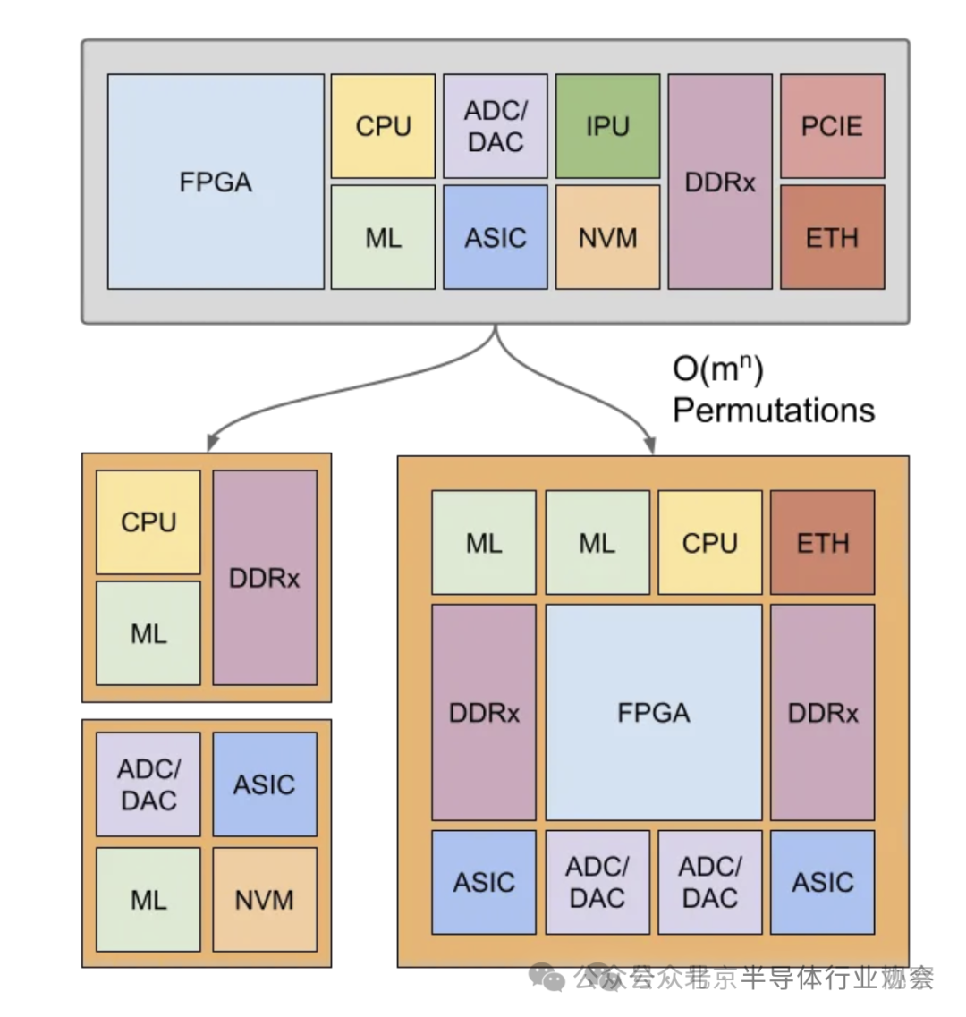
As illustrated, Zero ASIC is constructing the world’s first composable chip platform, capable of assembling billions of unique silicon systems from a ready-made chip catalog in hours, featuring:
Standardized chips – the first demonstration of fully standardized chips, supporting O(m^n) system arrangements (m = library size, n = socket count). Smart substrates – active 3D silicon substrates separate computation and networking, enabling Lego-like system composition. World-leading energy efficiency – chip communication efficiency below 0.1 pj/bit.
This scalable processor IP generator platform can quickly generate customized FPGA, CPU, NOC, and DSP for each application to meet the most stringent system requirements.
Automation – 100% automatic IP generation at the push of a button; Scalability – performance scalable from edge to data center. Maturity – our IP generator has been used for tape-outs of chips at 65nm, 28nm, 16nm, and 12nm.
To lower the barrier for custom ASICs, Zero ASIC has developed the open-source hardware compilation platform SiliconCompiler.
Field-tested – a silicon-validated process supports a wide range of open-source and proprietary EDA tools and PDKs. 24-hour tape-out cycle – optimized cloud-scale build infrastructure enables rapid design cycles. Deterministic – standardized lists and design-as-code methods ensure compilation determinism. Open-source – no lock-in or hidden agendas!
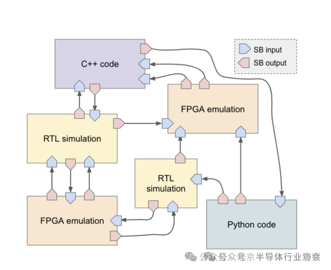
The company’s Switchboard digital twin platform enables near-real-time simulation, allowing teams to optimize system hardware and software before committing to expensive manufacturing cycles.
Fast – compared to leading commercial simulators, our chip-optimized digital twin platform can improve build and run times by an order of magnitude. Scalable – our latency-insensitive characteristics enable wafer-level designs and larger-scale designs. Flexible – standardized model interfaces facilitate seamless transitions between high-level models (e.g., QEMU), cycle-accurate RTL simulators (e.g., Verilator), and hardware-in-the-loop systems (e.g., AWS F1 FPGA).
In their view, this product will reshape ASIC design:
Step 1: Simulation – optimize hardware and software using the Digital Twin platform. Step 2: Prototyping – build prototypes based on fast small chips. Step 3: Optimization – optimize chip composition based on market feedback. Step 4: Market entry – place production orders and begin manufacturing.
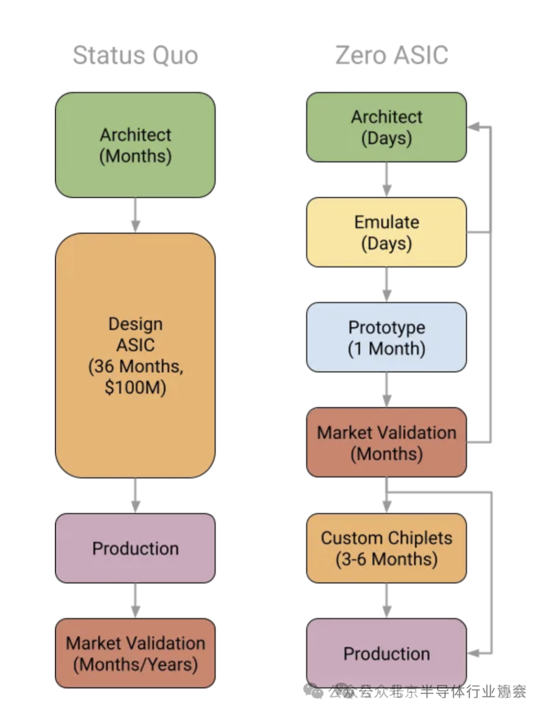
Finally, profit!
As they say, obsolescence is a critical issue for FPGA-based systems in aerospace, defense, healthcare, communications, automotive, and industrial applications, with lifespans ranging from 10 to 50 years. For example, the development of the F-35 fighter jet began in 1997 and did not reach full production until 2021. During this time, transistor density increased by 10,000 times, and the FPGA industry introduced six generations of new architectures. This mismatch between the continuous evolution of semiconductor technology and the slow infrastructure development cycle has led the U.S. military to estimate obsolescence-related NRE costs of $50 billion to $70 billion, with 15% of all replacement semiconductor parts being counterfeit.
Since the advent of FPGAs in the 1980s, commercial FPGA products have become increasingly complex, less standardized, and less transparent, exacerbating issues related to part obsolescence and counterfeiting. At best, the discontinuation notice for FPGA devices or eFPGA IP cores requires a complete redesign of the entire subsystem. At worst, this can lead to the termination of entire programs.
The next logical step to address FPGA obsolescence and counterfeiting issues is to move away from single-source components and establish a set of open-standard FPGA architectures, similar to the successful standards created for memory and passive components.
Over the past 25 years, there have been multiple attempts to open FPGA. In May 1997, the open-source FPGA research platform VPR was launched, helping to lower the barrier for high-quality, repeatable FPGA research. Unfortunately, VPR remains just a research tool, and commercial FPGAs still lack a fully open RTL-to-gate flow.
To address the lack of fully open FPGA devices, DARPA funded the OpenFPGA and PRGA FPGA generator research projects in 2018. While these open-source generators facilitated the tape-out of several academic chips, the final designs were neither standardized nor commercialized.
To circumvent the opacity of FPGAs, different approaches have been taken to reverse-engineer commercial FPGAs. However, as FPGA complexity has surged with Moore’s Law, this task has become increasingly difficult and expensive.
Despite these efforts, there is still no open, standardized commercial FPGA product on the market as of now.
With the launch of the Platypus eFPGA series, Zero ASIC has taken a significant step towards standardizing FPGAs by publicly releasing the complete architectural description and bitstream format of its commercial Z1000 eFPGA IP under the open-source Apache license, aiming to establish it as an open standard.
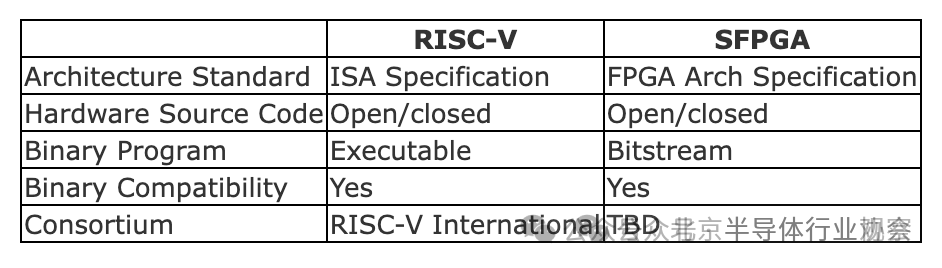
Historically, open standards have proven to be an effective way to prevent obsolescence and predatory pricing strategies. Notable ubiquitous open hardware standards include RISC-V ISA, IEEE Ethernet PHY, JEDEC memory, passive packages (e.g., 0603, 0805), PCIe, and USB. Like RISC-V, creating open standards does not mean that implementations must be open-source. The table below illustrates the similarities between the successful RISC-V ISA standard and the proposed FPGA approach.
The RISC-V ISA was initially an unassuming research project at the University of California, Berkeley, with the first specification released in 2011. In 2014, David Patterson and Krste Asanovic made a compelling case for why the ISA should be free, sparking the RISC-V movement. A decade later, RISC-V now ships in billions of devices annually.
“Developing an open-standard FPGA architecture and a standards-compliant component ecosystem will fundamentally change FPGA-based system design, just as RISC-V changed CPU design. Like RISC-V, market dynamics will determine whether the potential advantages of open standards can overcome the inertia of vendor lock-in.” — Andreas Olofsson said.