1
Introduction
The previous article reviewed the hierarchical methods of low power design【Technical Review】, and this article further discusses some of the key points. This is particularly beneficial for those who are new to low power design, as it may provoke more thoughts.
2
Why Low Power Design is Necessary
The previous article mentioned several reasons:
Heat Dissipation Costs: During the operation of a chip, electrical energy is consumed in the form of heat. To ensure the chip operates at a normal temperature, increased power consumption raises the requirements for packaging technology and heat dissipation methods, thereby increasing the heat dissipation costs of the chip;
Size: Increased power consumption necessitates larger heat dissipation devices, which in turn increases the size of the chip product;
Power Supply Costs: Increased power consumption shortens the effective battery life of end devices;
Reliability: Increased power consumption raises the environmental temperature of the chip, which can reduce the chip’s reliability;
Question: “Assuming it is not a mobile device or the battery has unlimited power, is low power design still necessary?”
Consideration: All semiconductors have a specified safe upper limit for junction temperature (TJ), usually around 150°C (sometimes 175°C). The lifespan of a semiconductor is inversely proportional to its operating junction temperature. Simply put, the lower the IC temperature, the longer its potential lifespan. Excessively high temperatures may lead to thermal breakdown. Therefore, to ensure the reliability of the chip, it is necessary to guarantee that the internal temperature does not exceed a certain limit, which must be ensured through design, packaging, and heat dissipation.
Packaging: High power consumption requires packaging materials with better thermal conductivity; ceramic packaging has better thermal conductivity than plastic packaging, but it is also more expensive.
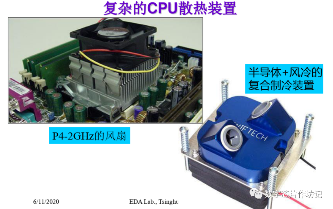
Size: Increased power consumption necessitates larger heat dissipation devices, which increases the size of the chip product. Heat dissipation devices include heat sinks, fans, and semiconductor + air cooling composite cooling devices, as shown in the figure below:
Therefore, as transistor density increases, it becomes increasingly important to implement low power design from the outset.
3
Basic Principles of Low Power
Power consumption consists of dynamic power and static power:

The charging and discharging model of a CMOS transistor is as follows:
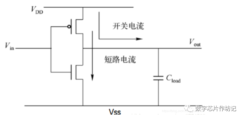
Question: How does the output capacitor change when the input Vin changes from 1 to 0? How does the power consumption change?
Consideration: When Vin is 1, the NMOS transistor is on, and the PMOS transistor is off, resulting in an output Vout of 0, meaning the voltage across the load capacitor Cload is 0. When Vin changes from 1 to 0, the PMOS transistor turns on, and the NMOS transistor turns off, effectively charging the capacitor with Vdd. After charging, Vout equals Vdd, and the charge on the capacitor is Q = Cload * Vout. The power consumed is equivalent to the work done to charge the capacitor to the charge Q, or from another perspective, the energy stored in the capacitor is the power consumed by the power supply. The energy stored in the capacitor is calculated as follows:
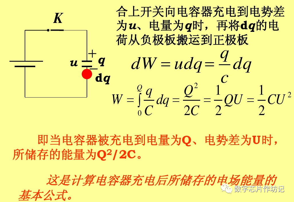
A capacitor with a potential difference of u and charge q stores energy as 1/2CVdd^2.
Additionally, the short-circuit current is positively correlated with Vth, meaning that increasing Vth can also reduce short-circuit current.
4
Principles of Low Power Design
Low power design methods involve system-level, logic-level, and physical-level design hierarchies, with higher levels potentially yielding more effective power reduction. The following diagram provides an overview of methods for reducing power consumption at various abstraction levels (the diagram includes methods related to power optimization at each level).
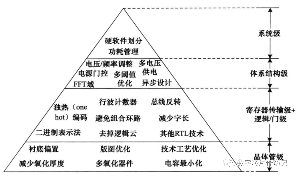
Principle 1. Design from the top down; the higher the design level, the better the optimization effect. Power optimization at the system level and architecture level can achieve 25% to 40%, while at the RTL level it may only optimize 10% to 25%, and at the gate level, it may only achieve 5% to 10%. Therefore, the earlier power optimization is performed, the better the results.
Principle 2.Look at the overall system from a global perspective while being meticulous about the details.
Principle 3.Balance power consumption, performance, and area; sometimes it is necessary to sacrifice performance for power consumption, requiring a compromise in design.
5
Common Design Methods
Multi-Voltage Supply: Multi-voltage supply for power management at the SoC level.
Multi-Vth: Use LVT threshold cells in critical paths and HVT/SVT cells in non-critical paths.
Power-Gating
Low Power Bus
Low Power Memory
Low Power Clock Network
Clock Gating: Although it seems simple, the code written sometimes lacks effective gating.
Software Optimization
Operand Isolation
Parallel Pipeline Structure
6
Reducing Switching Rate at the Structural Level
1. Question: Why can parallel structures reduce power consumption?
Consideration: Because parallel structures can reduce frequency, assuming the original frequency is f, two parallel paths can reduce the frequency to f/2, which means the voltage can be reduced to V/2. After parallelization, the area increases to twice the original, but from the power consumption formula CV^2f, the power consumption will be halved.
2. Question: Can pipelined structures reduce power consumption?
Consideration: “The path length is shortened to 1/M of the original path length. Thus, during one clock cycle, the charging/discharging of the capacitor becomes C/M. If the clock speed remains unchanged after adding the pipeline, then during one cycle, only C/M needs to be charged/discharged instead of the original C. Therefore, under the same speed requirements, a lower supply voltage can be used to drive the system.” In fact, pipelining is essentially a form of parallelism.
3. Reduce the logical depth of frequently switching gates.
4. Question: What is operand isolation?
Consideration: Operand isolation refers to adding a mux at the input when part of the logic does not need to output, thereby reducing the circuit’s switching rate and avoiding unnecessary transitions of operand inputs.
5. Question: What are the benefits of clock gating technology?
Consideration: On one hand, it reduces the internal power consumption of registers; on the other hand, it reduces the power consumption of the clock network, which can account for a significant portion, between 20% and 60%. It can also reduce the area of common muxes.
Clock gating is crucial in identifying the enable signals that accompany the signal, and it is also important to remember that the datapath can utilize clear enable signals for gating when data is invalid.
Additionally, I recommend an article titled “Global Top Chip Experts Reveal the Truth About Low Power Chip Design”; interested readers can click to read the original text.
Regardless of the distance, a gesture of appreciation is always welcome; how about clicking “Like”?● END ●

If you found this helpful, please click “Like”