1. IntroductionLet’s take a look at a diagram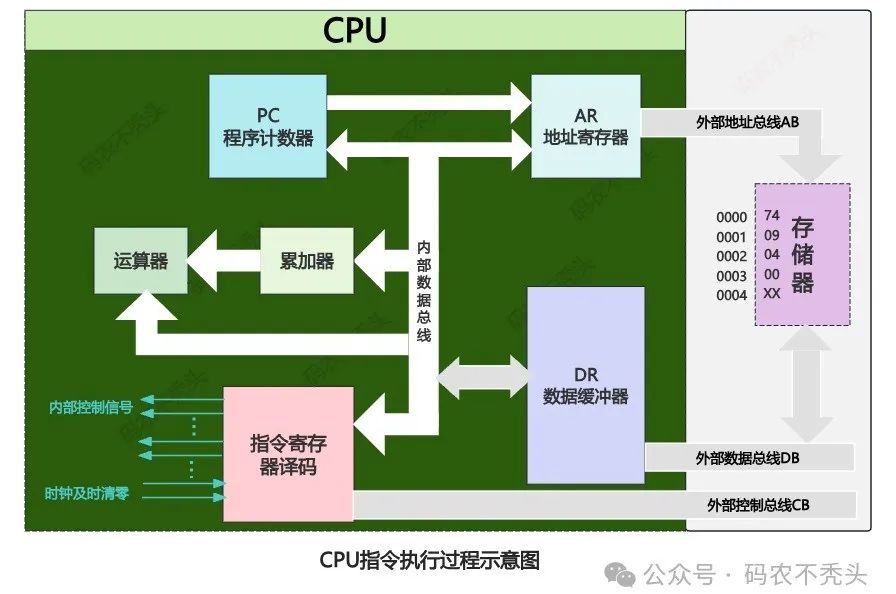 Friends who have read the previous blog post “The Execution Process of CPU Instructions” should have noticed that there is an indispensable component in the execution process of instructions in a computer, which is the bus. The diagram above shows multiple buses, and today we will introduce in detail the “highway” of computers: the principles and structure of the bus.2. Basic Concepts of Buses
✅ Bus ≠ Wires
Many people mistakenly believe that a bus is just a collection of wires. However, its complexity lies in the fact that it is a design specification: it includes hardware interfaces, communication protocols, timing logic, conflict resolution mechanisms, etc. All devices must “follow the rules” to share this channel.
✅ What is a Data Bus?
In the article discussing CPU architecture, we learned that the CPU has many registers, and the input and output terminals of these registers often need to be connected to a set of transmission lines for information transfer between them. Since registers are composed of flip-flops, and flip-flops only have states 0 and 1, generally, each signal transmission line can only carry the information of one flip-flop (0 or 1). If a transmission line can connect to one flip-flop and disconnect to connect to another, then a single information transmission line can time-share the information of multiple flip-flops. Similarly, a set of transmission lines can transmit information from multiple registers. We call this set of transmission lines a “bus“.
✅ How are Registers Connected to the Bus?
To achieve this functionality, additional circuits need to be added to each flip-flop that makes up the register. The tri-state output circuit (also known as the tri-state gate) is designed to achieve this purpose.
The tri-state output circuit can be composed of two NAND gates and two NMOS transistors (T1, T2) and one NOT gate, as shown in the diagram below:
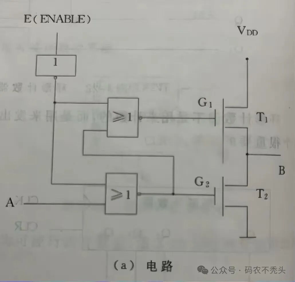
This is a circuit diagram; if you have seen the article on transistor principles, you should be able to understand it. The left side is the logic circuit of the NAND gate, and the right side has two transistors. If you don’t understand it, that’s okay; after all, we are not studying circuits. This circuit diagram is represented in logic symbols as shown below, which is the logic symbol of the tri-state output circuit.
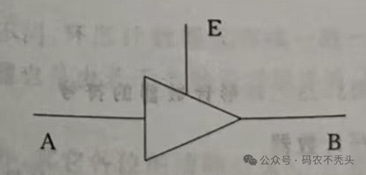 This circuit diagram will not be detailed here; I believe everyone is not interested. In summary, A and E are the input terminals, and B is the output terminal. When the input terminal E is at a high level, both possible levels of A (0 and 1) can be successfully transmitted to the output B, that is, when E=1, B=A; when the input terminal E is at a low level, terminals A and B are not connected, meaning there is a high-impedance state between them.The logic table for the tri-state output circuit is as follows:
| E | A | B |
| 0 | 01 | High-ZHigh-Z |
| 1 | 01 | 01 |
(The tri-state gate (E gate) and load gate (L gate) can be added to any register circuit (including counters and accumulators). Such registers are called tri-state registers. The L gate only controls the loading of data into the register, while the E gate only controls the output of data from the register.
With the L gate and E gate, we can utilize the bus structure to simplify the information transmission lines of the computer, making the design of the controller more reasonable and easier to understand.

As shown in the figure, there are four registers A, B, C, and D, each having L gates and E gates. Assuming their data width is 4 bits, only four data lines (regardless of how many lines, uniformly represented by thick lines labeled with numbers) are needed to communicate information between them.
3. Classification of Buses
Buses are generally classified into three categories based on the connected components: on-chip buses, system buses, and communication buses.
3.1. On-Chip Buses
On-chip buses refer to the buses within a chip, such as the connections between registers and between registers and the Arithmetic Logic Unit (ALU) within the CPU chip.
2. System Buses
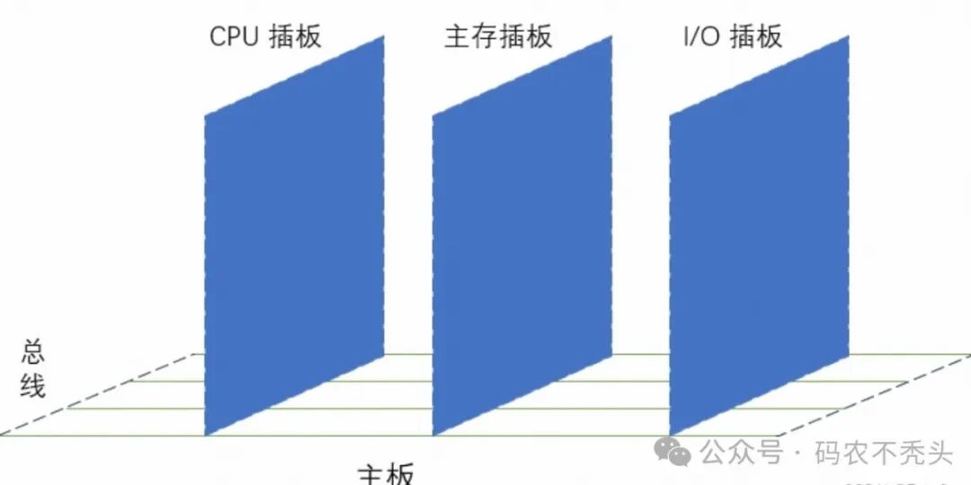
System buses refer to the information transmission lines between the CPU, main memory, and I/O devices. Since these components are usually placed on the motherboard or various plug-in boards (cards), they are also called board-level buses or inter-board buses. Physically, they are composed of many wires directly printed on the circuit board, extending to each component.
In the system bus, based on the different types of information transmitted, it can be further divided into three categories: data bus, address bus, and control bus.
(1) Data Bus
The data bus is used to transmit data information between functional components. It is a bidirectional transmission bus, and its width is related to the machine word length and storage word length, generally being 8 bits, 16 bits, or 32 bits.
The width of the data bus is an important parameter for measuring system performance. If the width of the data bus is 8 bits and the instruction word length is 16 bits, then the CPU must access the main memory twice during the instruction fetch phase.
(2) Address Bus
The address bus is mainly used to indicate the address of the source or destination data on the data bus in the main memory storage unit or I/O device.
The binary code on the address bus represents an address output by the CPU and is transmitted unidirectionally. The number of address lines is related to the number of storage units.
(3) Control Bus
The control bus is used to transmit various control signals.
Since the data bus and address bus are shared by all components connected to the bus, to allow each component to occupy the bus at different times, the control bus is needed to complete the allocation and scheduling.
Typically, for any control line, its transmission is unidirectional. However, for the control bus as a whole, it can be considered bidirectional. For example, the CPU can send read/write control signals to the main memory and I/O devices, and it can also receive interrupt requests from external devices.
3.3. Communication Buses
This type of bus is used for communication between computer systems or between a computer system and other systems (such as control instruments, mobile communications, etc.).
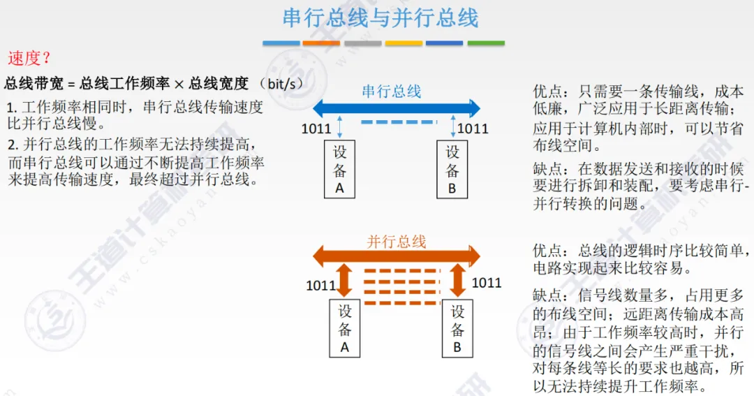
Communication buses are usually divided into two types based on the transmission method: serial communication and parallel communication.
Serial communication: refers to data being transmitted one bit at a time in sequence over a single 1-bit wide transmission line.
Parallel communication: refers to data being transmitted simultaneously from the source to the destination over multiple parallel 1-bit wide transmission lines.
Parallel communication is suitable for short-distance data transmission, usually less than 30m; serial communication is suitable for long-distance transmission, which can range from a few meters to thousands of kilometers. The data transmission rate of communication buses is generally inversely proportional to the distance.
4. Bus Structures
Bus structures can generally be divided into single bus structures and multi-bus structures.
4.1. Single Bus Structure
The single bus structure connects the CPU, main memory, and I/O devices (via I/O interfaces) to a single bus, allowing direct information exchange between I/O devices, between I/O devices and the CPU, or between I/O devices and main memory.
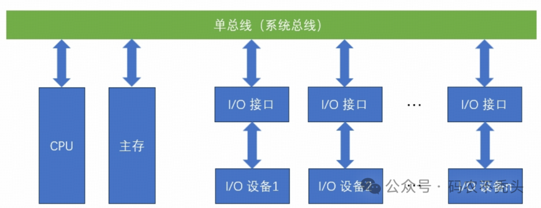
This structure is simple and easy to expand, but all transmissions go through this shared bus, which can easily create a bottleneck in the computer system. It also does not allow more than one component to transmit information to the bus at the same time, which inevitably affects the improvement of system efficiency. This type of bus is mostly used in small or microcomputers.
4.2. Dual Bus Structure
The dual bus structure is characterized by separating slower I/O devices from the single bus, forming a structure with separate main memory bus and I/O bus.
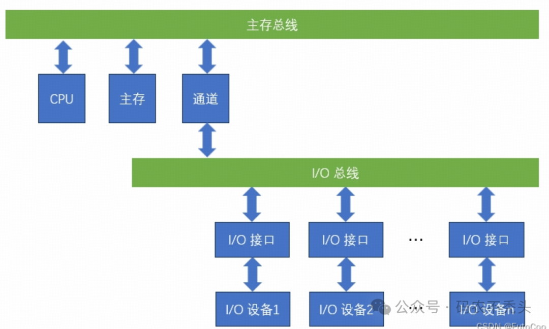
The channel is a processor with special functions, where the CPU delegates some functions to the channel, allowing the channel to manage I/O devices uniformly; this way, data transfer between external devices and main memory can be completed directly without going through the CPU, significantly increasing the system’s throughput. This structure is mostly used in large and medium-sized computer systems.
4.3. Triple Bus Structure
If I/O devices with different rates are further classified and connected to different channels, the efficiency of the computer can be further improved. This has led to the development of the triple bus structure.
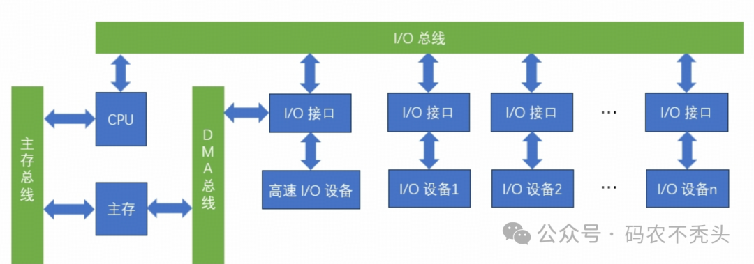
The main memory bus is used for transmission between the CPU and main memory; the I/O bus is for information transfer between the CPU and various I/O devices; the DMA bus is used for direct exchange of information between high-speed I/O devices (disks, tapes, etc.) and main memory. In the triple bus structure, only one bus can be used at any given time. The main memory bus and DMA bus cannot access the main memory simultaneously, and the I/O bus can only be used when the CPU executes I/O instructions.
If the data exchange of the cache is also considered, different triple bus structures can be constructed, and even a quadruple bus structure can be further developed.
4.4 Quadruple Bus Structure
Further development has led to the quadruple bus structure: CPU bus, system bus, high-speed bus/expansion bus.
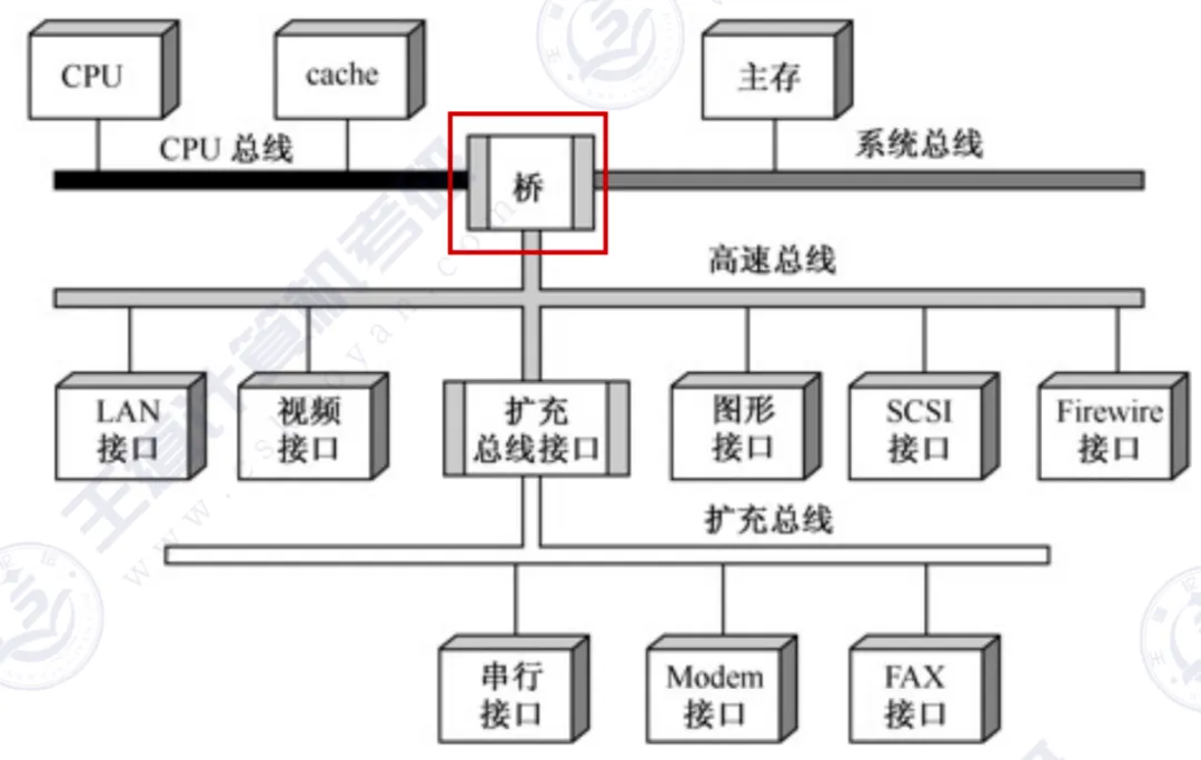
As shown in the red box in the figure, the quadruple bus structure adds bridges for bus connections.
5. Impact of Data Bus on Computer Performance
The performance of the data bus directly affects the overall performance of the computer system, mainly reflected in the following aspects:
-
Bandwidth: The bandwidth of the data bus determines the amount of data that can be transmitted in a unit of time.The larger the bandwidth, the faster the data transmission speed, and the higher the system performance.
-
Latency: The latency of the data bus affects the time required for data to be transmitted from one component to another.The lower the latency, the faster the system response speed.
-
Scalability: A high-performance data bus design can support more device connections, meeting the needs for system expansion.
Therefore, optimizing the design of the data bus is crucial for enhancing the performance of computer systems.
6. Challenges in Bus Structure Design
6.1 Data Coherence
In multi-core CPU or CPU+GPU architectures, multiple components may access the same memory address simultaneously. The bus structure must coordinate the data coherence issues between them.
For example, in a commonly used 4-core CPU, if CPU core A modifies variable X, cores B, C, and D must be immediately informed; otherwise, the memory value and cache value will become “split”. Software developers are aware of the importance of data coherence and how multi-threading ensures data coherence, such as using atomic classes, volatile keyword, synchronized keyword, etc. in Java to ensure data coherence. However, in reality, this relies on: bus arbitration mechanisms + MESI cache coherence protocol, which will be discussed separately later.
6.2 Electrical and Physical Limitations
As the bit width increases and frequency rises, the bus also faces challenges such as electromagnetic interference, signal reflection, and synchronization timing. Designers must consider:
-
Setup time
-
Driving capability and load capacitance
-
Bus length and terminal impedance matching
This is like a highway; designers must consider whether each vehicle can travel stably without collisions, rollovers, or delays.
7. Is the Bus Bottleneck Always Present?
You may ask: We have entered the 5GHz era; shouldn’t the bus no longer be a bottleneck?
In fact:
-
CPU performance is growing rapidly, butmemory/bus bandwidth is growing slowly
-
DRAM requires tens of nanoseconds for each access, while a CPU cycle is only 0.2 nanoseconds
-
In certain high-load scenarios,the CPU often “waits for memory”, rather than “waiting for instructions”
This creates what is known as:
“Memory Wall” – computational performance is limited by bus transmission.
As a result, engineers have to introduce:
-
Multi-level caches (L1, L2, L3)
-
Memory prefetch mechanisms
-
Advanced scheduling strategies such as bus throttling, bandwidth compression, etc.
8. Conclusion
Although bus technology may seem inconspicuous, it is a key factor in computer performance. In simple terms, the CPU’s computing power is the engine, and the bus is the transmission shaft that drives the system. Every breakthrough in performance bottlenecks often involves a reconstruction of the bus architecture.
Please open in the WeChat client
Afterthought: The more I write, the more knowledge I feel I need to convey. If there are topics you are eager to learn about, please leave a message in the comments, and I will prioritize those.
Please open in the WeChat client
Original content is not easy; if this article has helped you, please like, share, and follow our public account. Your recognition is my greatest motivation for creation.