 This article is compiled by the Semiconductor Industry Review (ID: ICVIEW) from semiengineering.
Edge AI, GenAI, and next-generation communications are adding more workloads to smartphones, which are already under pressure to deliver high performance with low power consumption.

Leading smartphone vendors are striving to keep up with the growing computational and power demands driven by localized generative AI, standard smartphone functionalities, and the need to move more data back and forth between the phone and the cloud.
In addition to edge features like facial recognition and other built-in applications, smartphones must adapt to continuously evolving communication protocols, systems, and applications. Moreover, they need to perform all these tasks on a single charge while remaining cool in the user’s hand or close to their face.
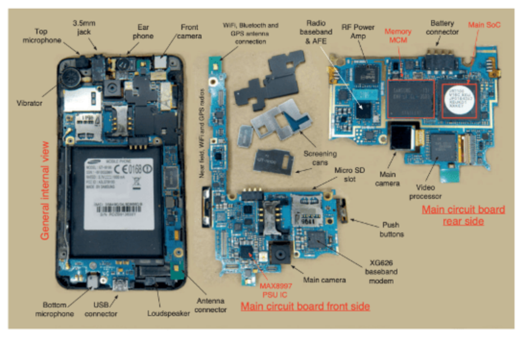
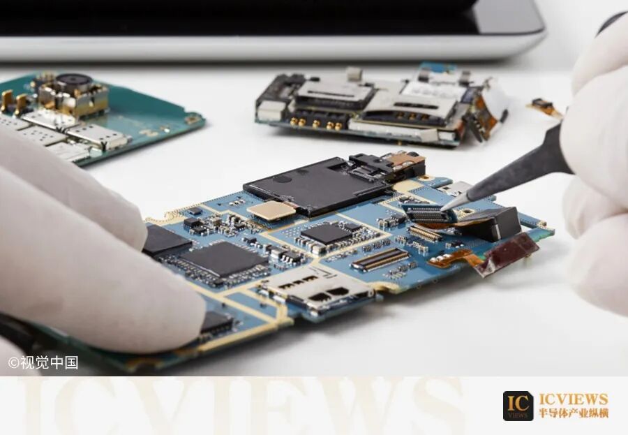
Figure 1: Smartphone circuit board, with the system-on-chip (SoC) shown in the upper right corner, containing an Arm CPU and other components. Source: Arm
Vitali Liouti, Senior Director of Product Management and Segmentation Strategy at Imagination Technologies, stated: “If you look at any high-end smartphone configuration, you will find that all SoCs adopt a heterogeneous architecture, composed of different modules that perform different functions but work together. From a system perspective, every mobile SoC manufacturer does this. They view the system in a heterogeneous way and consider it from a platform perspective (including both hardware and software).”
Amol Borkar, Director of Product Management and Marketing for Tensilica DSP at Cadence, mentioned that due to the rapid evolution of AI networks and the increasing diversity of AI model requirements, designing SoCs for the mobile market is becoming increasingly complex. “Unlike traditional workloads, AI models—especially large language models (LLMs) and Transformer variants—are constantly evolving in architecture, size, and computational requirements. This creates a moving target for chip designers who must hard-code support for future AI capabilities into silicon, which cannot be changed once manufactured. The challenge is further exacerbated by the need to support both ends of the AI spectrum—large-scale cloud-based models and compact, efficient models optimized for device inference (like TinyLlama). These smaller LLMs are crucial for implementing intelligent features on power- and memory-constrained mobile and embedded devices.”
In addition to keeping the SoC system perspective in mind, AI is also driving changes in individual processors and their task allocations.
John Weil, Vice President and General Manager of IoT and Edge AI Processors at Synaptics, stated: “The biggest changes happening right now follow two directions. CPU architectures in the Arm ecosystem and RISC-V are continuously being enhanced. People are adding vector math unit blocks to accelerate the various mathematical functions required by Transformer-based models. The second path involves enhancements to neural processors, which can be seen as GPUs but focused on accelerating edge AI models. These are primarily vector math units designed to accelerate various operands within models. If you look at the Arm Tensor Operator Set Architecture (TOSA) specification, you will find a variety of AI operands, and people are writing acceleration routines just like they would for GPUs using Open GL.”
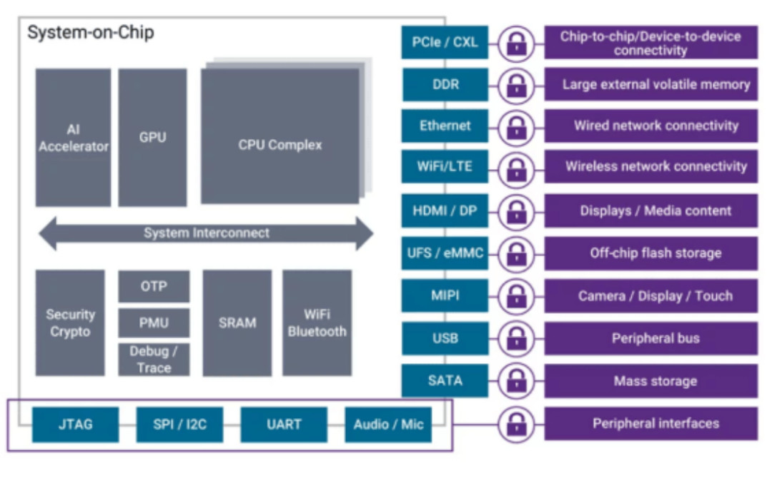
Figure 2: Mobile SoC design, where the AI accelerator can be another GPU, NPU, or high-end ASIC. Source: Synopsys
In recent years, the designs of GPUs and NPUs have been continuously updated to accommodate new use cases. Liouti from Imagination pointed out that GPUs typically occupy about 25% of the die area in high-end smartphone chips, while the size of NPUs is also increasing to handle substantial workloads. “Depending on the workload, the NPU may dominate, or you may need to break the problem down into certain layers for the NPU and certain layers for the GPU. NPUs have become an indispensable part of all low-power applications. For any application that needs to be always on, NPUs are the best choice. Additionally, you still need a powerful CPU because it requires a lot of initial work and management. If the CPU performance is poor, then no matter how large the GPU or NPU is, it won’t help.”
The key focus is on the energy efficiency of any form of parallel processing, whether it be graphics processing, general computing, or AI-specific computing.“We have been reworking our ALU engine and have thoroughly redesigned it to achieve very energy-efficient digital computations,” said Kristof Beets, Vice President of Technical Insights at Imagination. “The next step is to bring more NPU domain technologies into GPUs—data types are more specialized processing pipelines to provide sufficient performance. Furthermore, we need to achieve scalability across our entire customer base. We cannot overlook the developer community; how do we make it accessible? How do we ensure everything is plug-and-play? Then, how do we effectively optimize and tune them?”
Overall, integrating AI into chip design is becoming easier.“More than five years ago, people would say, ‘Oh my, I heard AI is coming. I don’t know what to do. Do I need to hire a team of data scientists to solve this?’ Maybe that was true ten years ago. But it is certainly not the case now,” said Steve Tateosian, Senior Vice President of IoT, Consumer Electronics, and Industrial MCUs at Infineon. “When it comes to developers, I have a team of PhD-level DSP engineers dedicated to debugging my audio front end. Now, perhaps you have a few—I’m not even going to call them AI engineers because they are just engineers—development engineers who know how to use AI tools to create these models. Over the past 5 to 10 years, the tools have significantly improved, including the workflows for engineers to acquire data, label data, create models, test models, and optimize models for deployment on end devices. Much of the specialized knowledge has been embedded into these tools, making it easier for a broader range of developers to create these applications or models.
 Everything is Visual, Wireless, and Tactile
As AI continues to evolve, there is a growing tendency towards visual forms. This requires more powerful processing capabilities than traditional text formats.
Marc Swinnen, Product Marketing Director at Ansys, stated: “In the past, interfaces were computer or text-based. Now, everything is video or fully graphical interfaces, which demand more from computing. A lot of computation is used to manage video input and output—from screen input to 1080p output, and so on.”
Moreover, everything is wireless, leading to an increase in simulated content on smartphones.“Now there are about six antennas in a phone—it’s crazy,” Swinnen said. “All these high-frequency telecom functions, from Wi-Fi, 5G, Bluetooth to AirDrop, each have their own frequencies, chips, and antennas.”
The continuous evolution of communication standards presents further challenges for SoC designers.
“The most important thing is to realize AI use cases and drive UFS implementation, accelerating the standardization process,” said Hezi Saar, Executive Director of Product Management for Mobile, Automotive, and Consumer IP at Synopsys and Chairman of the MIPI Alliance. “The MIPI Alliance is able to bring it forward by a year, which indeed reduces risk. People are defining it now. SoC and IP vendors need to develop their IP while the specifications are being defined. They need to tape out and get silicon that meets part of the specifications and plan for the next specification, planning for interoperability, and building ecosystems while we work. In the past, this was not the case. Specifications used to evolve at a certain frequency. There would be a specification every two years. But everything has been compressed because AI is more software-driven, which affects hardware. Hardware is not software.”
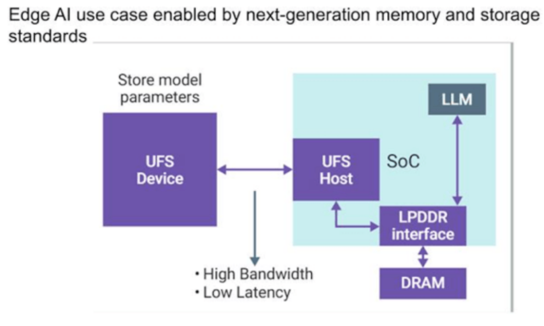
Figure 3: Use cases being implemented in smartphones, where LLMs or AI engines need to be available on storage devices. Source: Synopsys
Saar stated: “When you turn on the device, most of the model’s functionality needs to find itself in DRAM, which means that the read connections from the UFS device to the SoC need to be very efficient. This is latency. You can’t press a button, ask a question, and then wait two seconds. Of course, there are more ways to do this. You don’t need to read everything. You can do partial reads. But all these systems store data here, and I need to push it quickly to DRAM. I let the LLM run, say, an on-chip accelerator. But I need to connect it to DRAM for computation and then return it to the user so they can listen to audio. In mobile devices, it must be very, very efficient. Power consumption is extremely important. They will reduce transmission. I will put the UFS device to sleep as much as possible. I expect storage connections and DRAM connections to continue to evolve very quickly—much faster than before.”
The rise of multimodal models and GenAI tools (such as Stable Diffusion) further complicates matters, as these tools integrate text, image, and audio processing into a unified architecture. Borkar from Cadence stated: “These models require flexible and efficient computational structures capable of handling various data types and execution modes. To remain resilient in the face of uncertainty and rapid AI evolution, the design of AI subsystems must consider future developments. This often involves integrating programmable IP modules with NPUs, allowing SoCs to adapt to new model architectures and workloads post-tape-out. To support such a wide range of AI use cases, SoCs need to be not only powerful and efficient but also architecturally agile, making AI-centric chip design one of the most dynamic and challenging frontiers in mobile computing.”
Another use case for mobile algorithms is determining what constitutes a meaningful touch on the screen, whether it be for “slab” phones or foldable phones, which face additional challenges due to their very thin screens.
Sam Toba, Product Marketing Director at Synaptics, stated: “As the display becomes thinner, the top touch layer must be closer to the noise-prone display layer. We have to deal with a lot of display noise from individual pixels. This is a problem for very, very thin displays. Because the background layer is very thin, the capacitance becomes higher due to the decreasing distance between the plates. This is a big issue because when you sense a touch, the capacitance it senses is very small, while the background capacitance is very large, making it more difficult to identify valid finger signals from such a large noise (capacitance noise) in thin panels.”
This ultra-low-power chip needs to determine which signals are meaningful before waking up the host SoC. “If the host has to detect touches, just searching for touch signals will consume a lot of power, meaning the device must always be on. Most touch signals must be rejected.”
Local Processing of AI Features and Models
Smartphones are equipped with numerous AI applications, and the number is continuously increasing. Swinnen from Ansys pointed out that processing should be done on the phone whenever possible, so that only streamlined information is sent to the cloud. For example, machine learning functions like facial recognition or photo editing should be processed close to the camera.
Inference requests for GenAI models (such as ChatGPT or agent AI assistants) can also be processed locally. Saar from Synopsys noted that AI models have become more efficient and compact, so whether they are a few megabytes, kilobytes, or gigabytes, they can be stored on devices, depending on the model and device in question.
Local processing on devices has numerous advantages.Ron Squiers, Solutions Network Expert at Siemens Digital Industries Software, stated: “By embedding AI hardware into these mobile devices, they can perform large language model inference internally. There is no need to send transactions back to the cloud for heavy inference; it can be done at the edge. This has dual benefits: lower latency, better real-time response, better closed-loop servo control, and better protection of data privacy generated locally at the edge.”
Others agree with this point.“You don’t have to send data to the cloud, so power consumption and costs are reduced,” said Tateosian from Infineon. “Some edge AI applications can enhance intelligence without increasing connectivity costs or can reduce the number of connections. This means reducing cloud connections and lowering power consumption for end devices.”
Liouti from Imagination stated that in the era of ultra-optimization, designers need to minimize technical debt to maximize the potential and performance of smartphones. “Data movement accounts for 78% of power consumption. Our main focus is on ‘how do we reduce this data movement?’ This can be achieved at the GPU level, which is also our focus, but it can also be achieved at the platform level and SoC level. We must develop extremely advanced technologies to reduce data movement, and this becomes more complex for neural networks—especially for large neural networks, as they require a lot of data.”
While more device-side AI processing is happening, some functionalities will still run in the cloud due to battery and power constraints. “You always need to make trade-offs,” Liouti said. “This is just the beginning of a great journey; things will be very different in a few years. We are just scratching the surface. I believe Transformers are the foundational modules for building grander goals. Right now, we need to distinguish hype from reality. Take the image generation models currently running locally on mobile devices as an example. The reality is that their performance is far inferior to the models you find using Midjourney on a computer. Things will change in a few years.”
More powerful GPUs will be part of the solution. “In the mobile space, we can convert additional power savings into higher clock frequencies and better performance because we can maintain the same power and thermal budget,” said Beets from Imagination.
However, Tateosian from Infineon observed that after each new version release, the user experience on smartphones has not changed significantly. “Despite the improvements in performance and memory of these devices, the software is consuming them.”
Conclusion
Several key trends are driving the transformation of mobile SoC design.Ansys’s Swinnen stated: “The rise of simulation technologies, the booming of video and AI, and today’s applications’ demand for high-performance computing (HPC) require chips to have powerful computing capabilities. These factors are driving the development of SoCs, but smartphone manufacturers are constrained by the need to maintain low power and small size, and they face greater economic constraints compared to GPU companies like NVIDIA. For them, performance is the most important; if the cost is slightly higher, they will accept it. But for mobile chips, cost is not the same. To achieve millions of units, cost must be kept low.”
Designers must ensure that SoCs are designed from both hardware and software perspectives. “Those who forget this will fail,” said Liouti from Imagination. “When considering language models, hierarchies, and operations, we must take this into account. It sounds simple, but it is not. Essentially, you must find the best way to leverage hardware for mathematical computations to ensure your solution is ahead of the competition, as we are competing with giants. You must conduct co-design of hardware and software, which cannot be done by a single engineer. It must involve multiple different disciplines, some of which may even be completely unrelated.”
*Disclaimer: This article is the original work of the author. The content reflects their personal views, and our reposting is solely for sharing and discussion purposes, not representing our endorsement or agreement. If there are any objections, please contact us.