FPGA Learning Notes: 1. Basics of Digital Circuits
This note records my learning process of FPGA, briefly documenting some knowledge points that may not be very clear or are worth recording for future reference.
If the content of the notes happens to help you, I am very happy!
1. What is a Digital Circuit
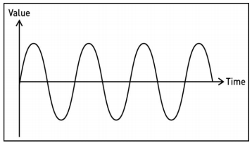
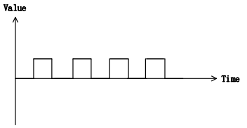
In life, there are two concepts: digital signals and analog signals. Analog signals generally include signals such as pressure, temperature, speed, etc., where the value of the analog quantity can change continuously over time. Digital quantities, on the other hand, refer to signals that do not change continuously over time, such as level signals.
Analog signal (left), digital signal (right)
In IC/FPGA logic design, generally only digital signals can be processed. Of course, some high-end FPGAs now integrate AD modules, which can also collect analog signals.
2. Number Systems
2.1 Introduction to Number Systems
The number system formats generally include binary, octal, decimal, and hexadecimal, with binary, decimal, and hexadecimal being the most commonly used.
The Verilog hardware description language is the mainstream language for IC/FPGA development, and the number format in Verilog is represented as follows:
• Binary (BIN format) is represented as:<span>4'b0101</span> which represents a 4-bit binary number 0101;
• Decimal (DEC format) is represented as:<span>4'd2</span> which represents a 4-bit decimal number 2 (binary 0010);
• Hexadecimal (HEX format) is represented as:<span>4'ha</span> which represents a 4-bit hexadecimal number a (binary 1010).
When the bit width and base of a number are not specified in the code, it defaults to a 32-bit decimal, for example, 100 actually represents<span>32'd100</span>.
Conversions between number systems can be done using the programmer mode of the Windows calculator.
2.2 Number System Conversion
The commonly used numerical expression is decimal, but binary is used in digital circuits. It is necessary to understand the conversion methods between decimal and binary.
2.2.1 Binary to Decimal
From right to left, multiply each binary digit by the corresponding power of 2 (starting from power 0), and then sum each result.
For example: binary converted to decimal
Then the corresponding decimal number for the binary is.
2.2.2 Decimal to Binary
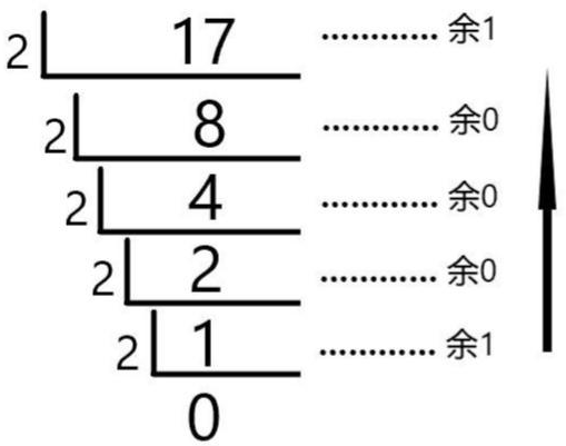
Use the “divide by 2 and take the remainder, reverse order” method.
Dividing the decimal integer by 2 gives a quotient and a remainder; then divide the quotient by 2 again to get another quotient and remainder, and continue this until the quotient is zero. The first obtained remainder becomes the least significant bit of the binary number, and the later obtained remainders become the most significant bits, arranged in reverse order to form the binary number.
For example: decimal converted to binary
Then the corresponding binary number for the decimal is.
For converting decimal to other bases, use the “divide (corresponding base) and take the remainder, reverse order” method.
2.2.3 Signed Binary
For example: binary converted to decimal
Unsigned:
Signed:
Signed binary numbers involve the concepts of original code, inverse code, and complement code, which can be learned from the links in the supplementary knowledge.
In computer memory, integers are stored in the form of complement code. This means that when reading integers, a reverse conversion is also required, which is to convert the complement code back to the original code.
Converting complement code to original code is also simple: first subtract 1, then invert the value bits.
For example: the signed binary number stored in the computer is in complement form, and converting it to original code involves two steps:
• First subtract 1, changing it to
• The first bit is the sign bit, 1 indicates the value is negative, the remaining bits represent the value, and inverting the value bits gives
Reading: the highest bit 1 indicates the value is negative, the remaining bits is the binary original code, converting to decimal gives 6, thus this signed binary number represents the value of.
2.3 Supplementary Knowledge
Detailed introduction to conversions between various bases, decimal to base conversions, one-hot code, BCD code, Gray code, error correction codes, parity codes, etc.:
2. Detailed explanation of number systems (integer part) – Mufeng Peninsula – Blog Garden (cnblogs.com)[1]
Detailed introduction to signed binary numbers, original code, inverse code, complement code, etc.:
3. Signed binary numbers (original code, inverse code, complement code) – Mufeng Peninsula – Blog Garden (cnblogs.com)[2]
For deeper reasons for using complement code and introduction to modular arithmetic, carry overflow:
Binary: Signed integer encoding and addition/subtraction operations // Lumin (lumin.tech)[3]
3. MOSFET
Metal-Oxide-Semiconductor Field-Effect Transistor (MOSFET) is a type of field-effect transistor that can be widely used in both analog and digital circuits.
In recent years, digital circuits have basically been composed of MOSFET field-effect transistors. A MOSFET is a semiconductor device that can work like a switch when a voltage is applied. There are two types of MOSFETs: P-type MOSFET and N-type MOSFET.
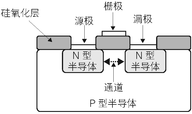
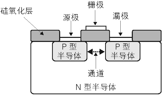
Structure of N-type MOSFET:
Structure of P-type MOSFET:
A MOSFET has three electrodes: source, drain, and gate. Functionally, the source, drain, and gate are used for current input, current output, and current control, respectively. The source and drain of a MOSFET use the same type of semiconductor material, while the channel under the gate is filled with a different type of semiconductor material. The source and drain of an N-type MOSFET use N-type semiconductor, while the channel under the gate uses P-type semiconductor. The material composition of P-type MOSFET is the opposite of that of N-type MOSFET.
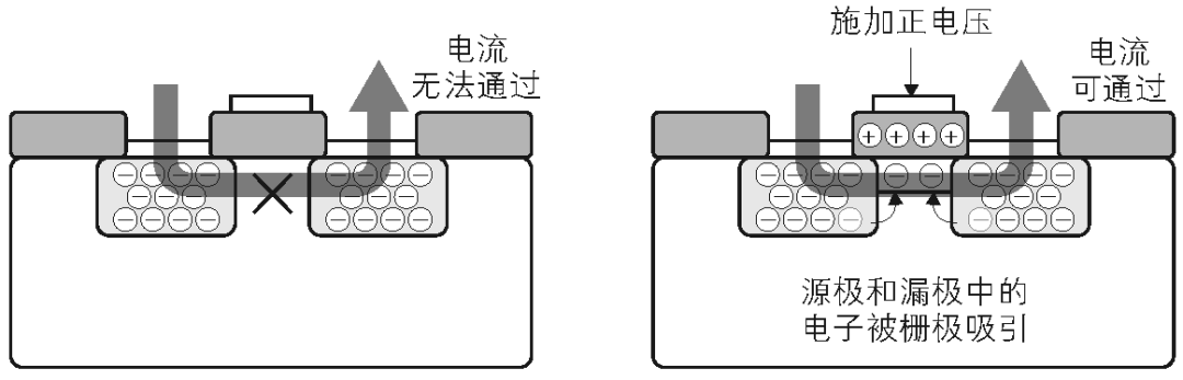
Taking N-type MOSFET as an example, its working principle is explained. When no voltage is applied to the gate, which controls the current, the source and drain are filled with different semiconductor materials, so current cannot flow. When a positive voltage is applied to the gate, the free electrons in the N-type semiconductor material between the source and drain are attracted by the gate, filling the channel with electrons, allowing current to flow between the source and drain.
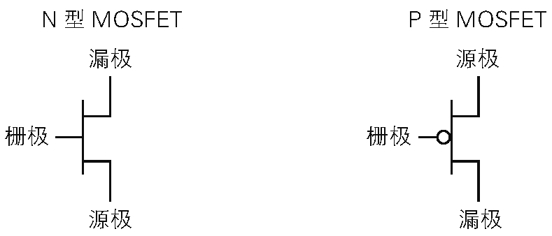
When a power voltage (H) is applied to the gate of an N-type MOSFET, current can flow; when grounded (L), current cannot flow. Conversely, when the gate of a P-type MOSFET is grounded, current can flow; when a power voltage is applied, current cannot flow. The complementary use of N-type and P-type MOSFETs forms a gate circuit called CMOS (Complementary Metal Oxide Semiconductor). CMOS can be used to create various logic circuits.
The circuit symbols for N-type and P-type MOSFETs are:
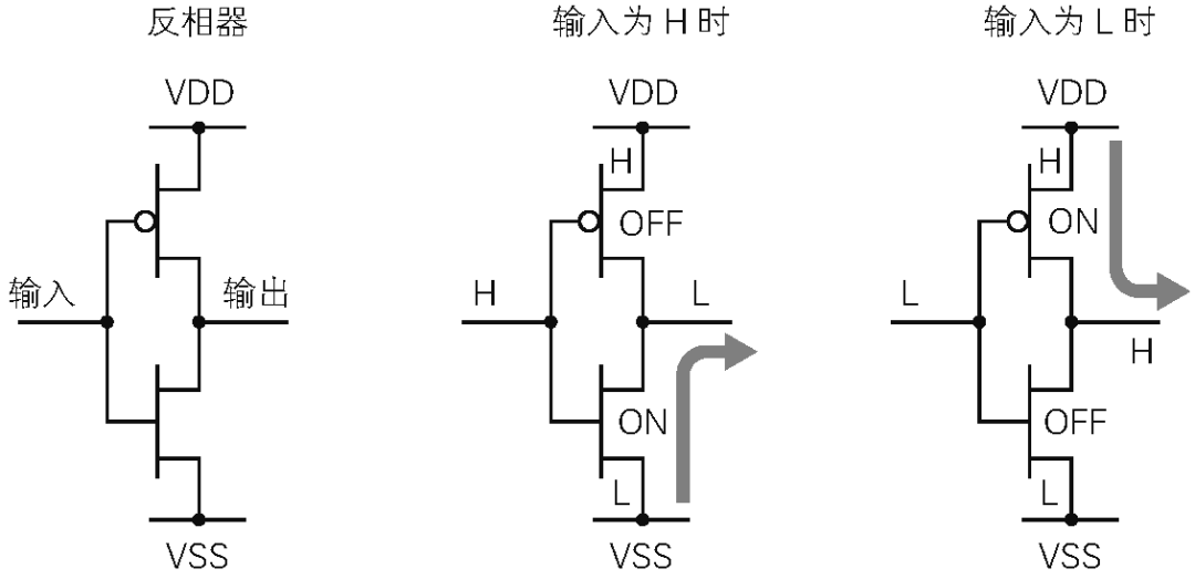
Combining MOSFETs as shown in the diagram below can achieve a NOT gate circuit. When the input is H, the N-type MOSFET turns on, and the output is L; when the input is L, the P-type MOSFET turns on, and the output is H.
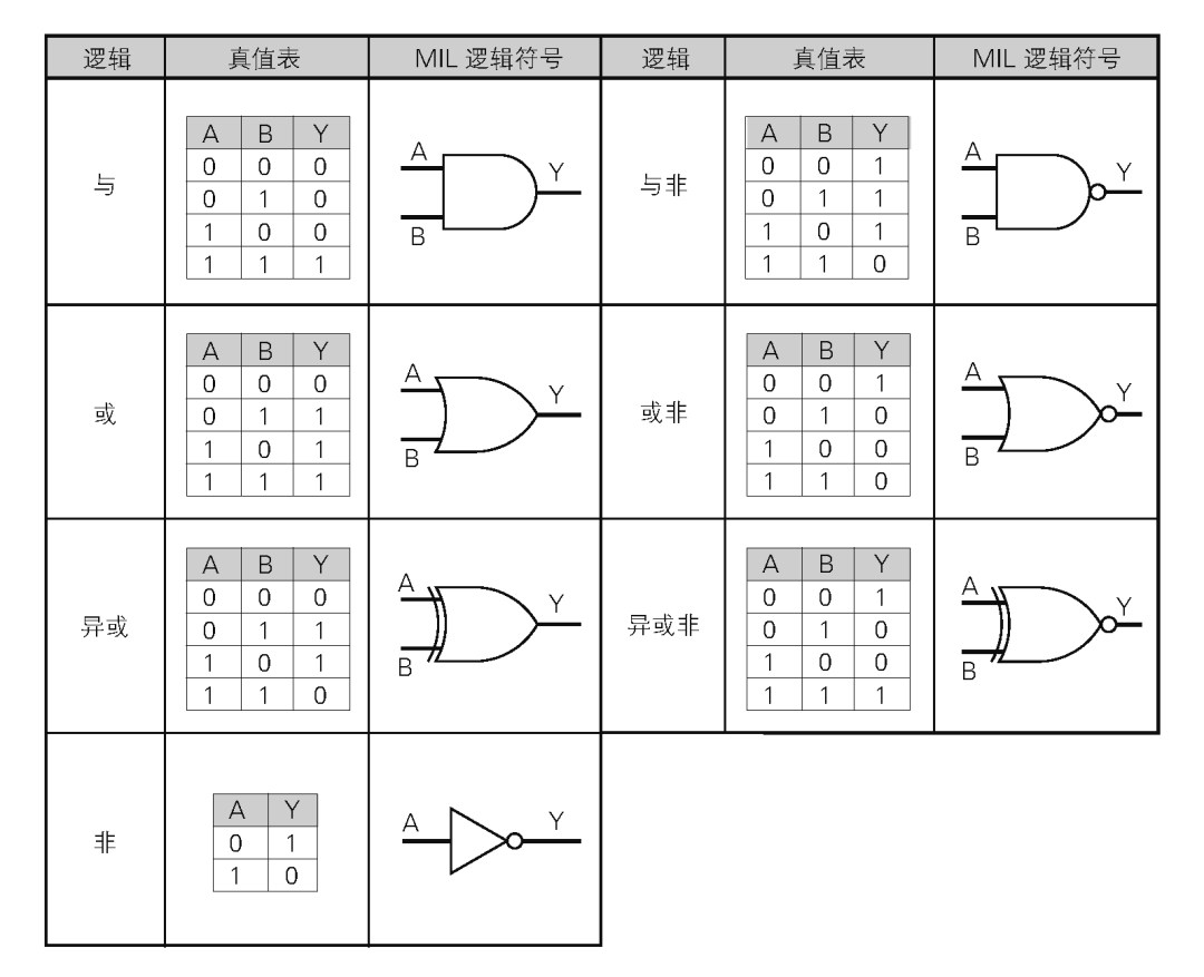
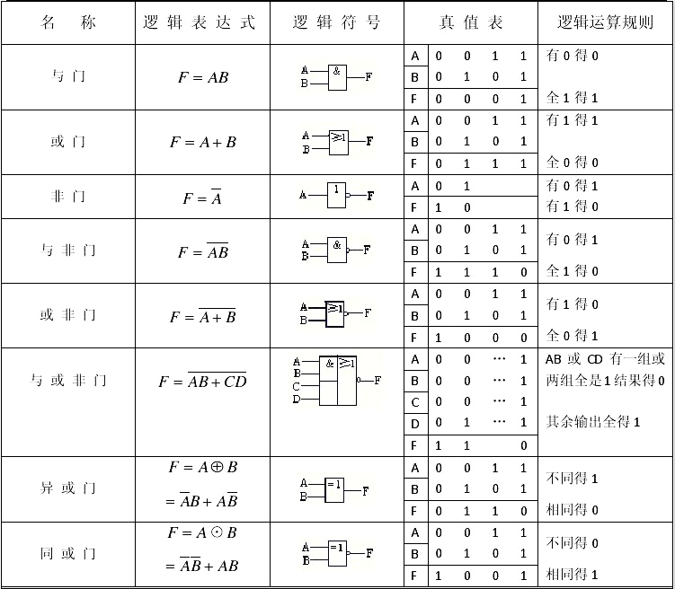
From the simplest NOT gate circuit to various logic gate circuits, all can be implemented by combinations of MOSFETs. The diagram below lists the basic logic gates defined in logic gate circuits. The circuit symbols for logic gate circuits are called MIL (Military Standard) logic symbols. Digital electronic circuits achieve various logic circuit functions through combinations of basic logic circuits.
4. Logic Gates
AND gate, OR gate, NOT gate, NAND gate, NOR gate, XOR gate, XNOR gate
5. Latch
A latch is essentially a bistable circuit that can stabilize in two different states and switch to another stable state under appropriate input. The state it is in is the information we want to store.
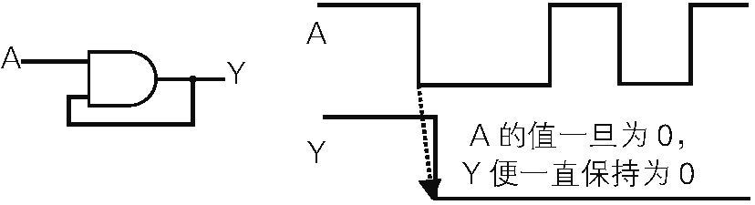
The diagram below shows a very simple latch, which consists of a 2-input AND gate and connects the output back to one of the inputs to form a feedback loop. Once the input A of this circuit is 0, the value in the feedback loop remains 0. This allows the feedback loop to store the logic value.
5.1 D Latch
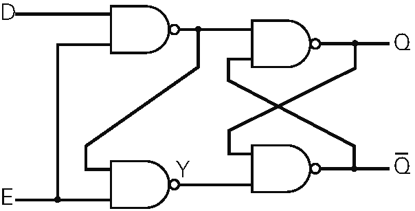
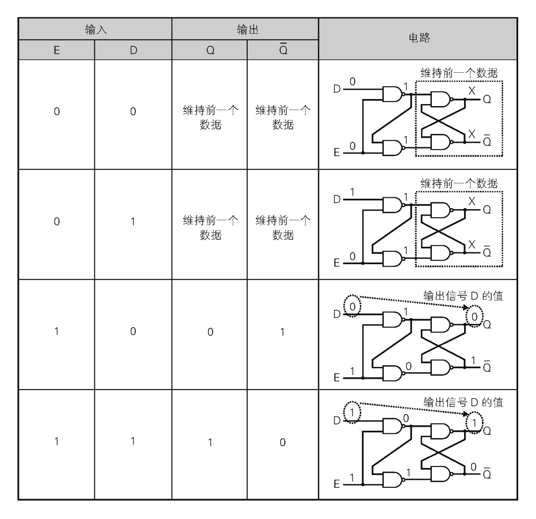
The circuit structure of the D latch is shown in the diagram below, consisting of 4 NAND gates. The D latch has two input signals D (Data) and E (Enable), and two output signals. The D latch holds the previous data when E is 0, and outputs the input D data to Q when E is 1. is the inverse signal of the output signal.
The truth table of the D latch is shown in the diagram below. Since the D latch directly outputs the input D when E is 1, it is also called a transparent latch.
5.2 Other Latches
Other latches include SR latches, JK latches, and improved D latches such as Earle latches, etc. Refer to:Digital Circuits: Construction Design of Latches/Flip-Flops – rvalue’s blog[4]
6. Flip-Flops
6.1 D Flip-Flop
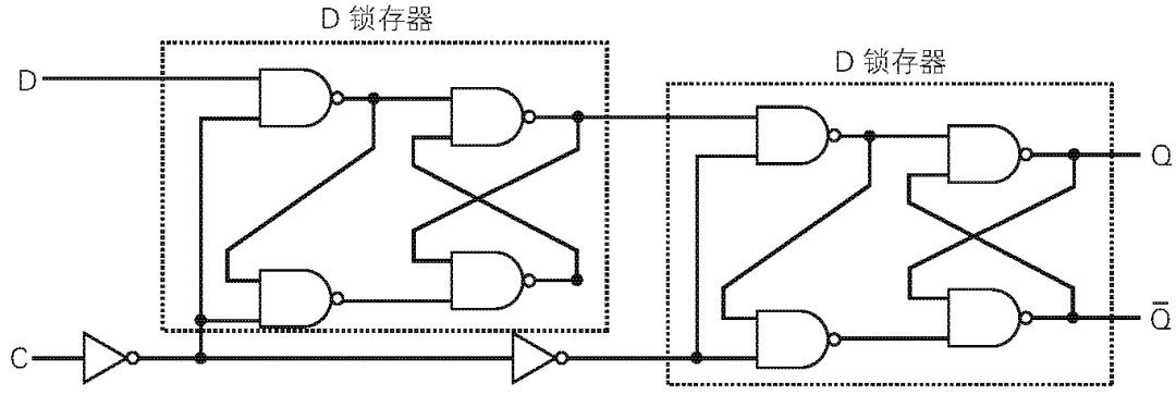
The D latch combined with a NOT gate can implement a D flip-flop that synchronizes and stores data based on the clock signal.
The circuit structure of the D flip-flop is:
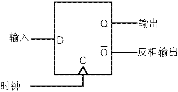
The circuit symbol of the D flip-flop is:
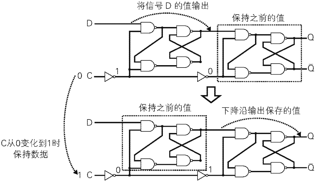
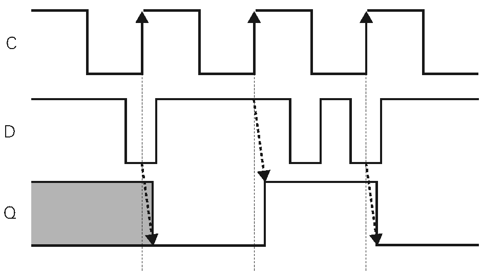
The D flip-flop has two input signals D (Data) and C (Clock), and two output signals. When the C of the D flip-flop is 0, the front D latch outputs the value of signal D, and the back D latch holds the previous data. When C is 1, the front D latch holds the previous data, and the back D latch directly outputs the data held by the front D latch through output.
The action principle of the D flip-flop is:
The waveform diagram of the D flip-flop is:
Due to its simple principle and structure, the D flip-flop is widely used in synchronous circuits.
Setup Time and Hold Time
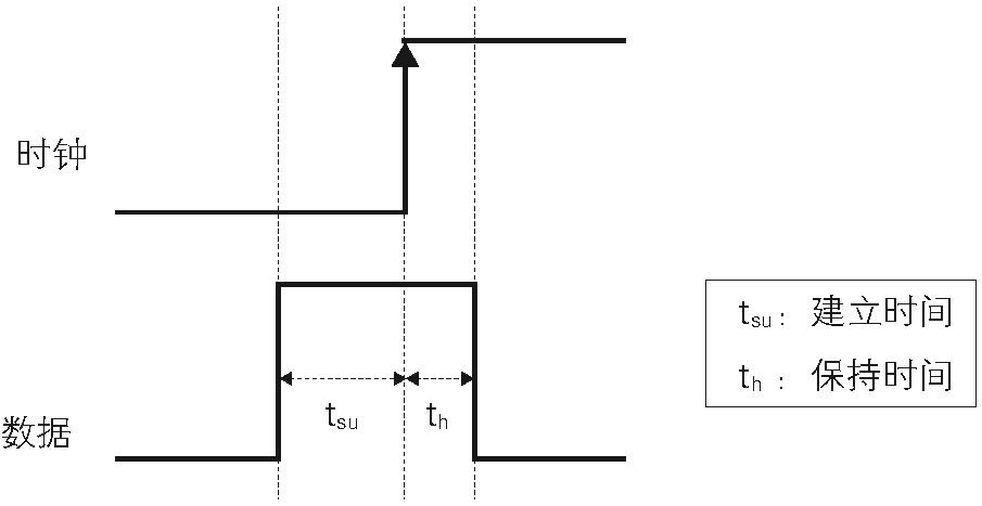
The D flip-flop is triggered by the edge of the clock signal to store data. Therefore, it is necessary to stabilize the input signal for a period of time before and after the clock edge. If the input signal changes during the clock transition, it may not store data correctly. Therefore, to allow the D flip-flop to store data correctly, two basic conditions must be met: setup time and hold time.
Setup time is the time during which the input signal must be stable before the clock changes, while hold time is the time during which the input signal must be stable after the clock changes.
The relationship between setup time and hold time:
By adhering to both setup time and hold time, the D flip-flop can store data correctly.
6.2 JK Flip-Flop
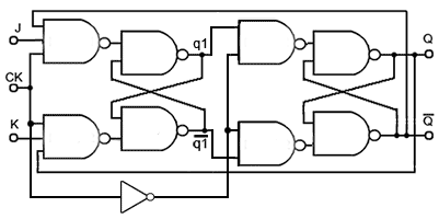
The JK flip-flop is similar to the JK latch but only responds to inputs on the clock edge. The JK flip-flop also has various implementation structures, one of which is a master-slave structure that is relatively easy to understand. Below is the circuit structure of a falling edge JK flip-flop:
When the clock is high, the master SR latch on the left temporarily holds and results, while the slave SR latch on the right keeps value unchanged. When the clock is at the falling edge and low, the inputs of the master SR latch are all high, essentially in a locked state, passing the results calculated at the falling edge to the downstream slave latch, which updates the value of.
In addition, the JK flip-flop can also be implemented based on the D flip-flop. According to the truth table of the JK latch mentioned above, we can simplify as follows:
Construct the corresponding gate circuit to calculate D and feed it to the D flip-flop.
6.3 T Flip-Flop
The T in T flip-flop stands for toggle. It has an input and a clock signal input. When the flip-flop is triggered, if, then set. Otherwise remain unchanged. Taking the rising edge trigger as an example, the truth table is as follows:
Clock
Action
X
Not rising edge
Hold
0
Rising edge
Hold
1
Rising edge
Toggle
After implementing the JK flip-flop, you can directly connect T to the J and K inputs of the JK flip-flop to achieve the above functionality.
7. Karnaugh Map and Logic Algebra Simplification Method
The content of the Karnaugh map and logic algebra simplification method includes algebraic simplification methods (basic laws, basic principles, etc.) in combinational logic circuit design and Karnaugh map simplification methods (including tool software, practical cases) – Juejin (juejin.cn)[5]
8. Competition and Hazard
8.1 Causes
When a variable reaches the output throughmore than two paths, due to the different delay times on each path, the arrival times at the destination vary, a phenomenon known as competition.
In combinational circuits with competition, when a variable changes, if the logical relationship described by the truth table is temporarily disrupted, resulting in unintended spikes at the output (glitches), this phenomenon is called hazard.
8.2 Types and Judgments of Hazards
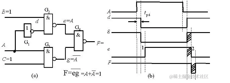
In the diagram (b), there is competition at points 1 and 2, but since it is a NAND gate, no hazard occurs at point 1, while a hazard occurs at point 2.
A variable appears in function F as both the original and inverted variable, indicating that the variable has competition conditions. If other variables are eliminated (set to 0 or 1), leaving the variable with competition, if the function appears=, a negative spike hazard occurs, known as “0” hazard; if the function appears=, a positive spike hazard occurs, known as “1” hazard.
8.3 Methods to Eliminate Hazards
• Modify the logic design
• Add redundancy to eliminate logical hazards
• Add selection signals to avoid glitches
• Connect a filtering capacitor at the output
Hazard pulses are narrow pulses, and connecting a capacitor of several hundred pF at the output can filter them out.
• Use Gray code: For example, in digital circuits, Gray code counters are often used instead of binary counters because Gray code outputs only one bit change at a time, eliminating the conditions for competition hazards.
• Use synchronous circuits: In synchronous circuits, signal changes occur at clock edges, and as long as glitches are not sampled at clock edges, they will be eliminated.
9. Others
There are also some other deeper or FPGA-related digital knowledge, such as:
• [FPGA] Basics of Digital Circuit Design_This task: Use Verilog to describe the n-bit basic register triggered on the rising edge, supplement the program in the right code window – CSDN Blog[6]
• Methods for converting between binary and decimal (simple and easy to learn!)_Binary to Decimal – CSDN Blog[7]
• Basic knowledge of digital circuits – Zhihu (zhihu.com)[8]
• 2. Detailed explanation of number systems (integer part) – Mufeng Peninsula – Blog Garden (cnblogs.com)[9]
• 3. Signed binary numbers (original code, inverse code, complement code) – Mufeng Peninsula – Blog Garden (cnblogs.com)[10]
• Binary: Signed integer encoding and addition/subtraction operations // Lumin (lumin.tech)[11]
• Practical knowledge of eight common logic gates (logic expressions, logic symbols, truth tables, logic operation rules) – Lincoln Park – Blog Garden (cnblogs.com)[12]
• Turing Community (ituring.com.cn)[13]
• Digital Circuits: Construction Design of Latches/Flip-Flops – rvalue’s blog[14]
• Metal-Oxide-Semiconductor Field-Effect Transistor – Wikipedia, the free encyclopedia (wikipedia.org)[15]
• Karnaugh map and logic algebra simplification method includes algebraic simplification methods (basic laws, basic principles, etc.) in combinational logic circuit design and Karnaugh map simplification methods (including tool software, practical cases) – Juejin (juejin.cn)[16]
Cited Links
<span>[1]</span> 2. Detailed explanation of number systems (integer part) – Mufeng Peninsula – Blog Garden (cnblogs.com): https://www.cnblogs.com/liuyz1996/p/14983943.html#6奇偶校验码检错码和纠错码<span>[2]</span> 3. Signed binary numbers (original code, inverse code, complement code) – Mufeng Peninsula – Blog Garden (cnblogs.com): https://www.cnblogs.com/liuyz1996/p/15008925.html<span>[3]</span> Binary: Signed integer encoding and addition/subtraction operations // Lumin (lumin.tech): https://www.lumin.tech/articles/bitwise-operations/<span>[4]</span> Digital Circuits: Construction Design of Latches/Flip-Flops – rvalue’s blog: https://blog.rvalue.moe/structure-and-design-of-latches-and-flip-flops/<span>[5]</span> Karnaugh map and logic algebra simplification method includes algebraic simplification methods (basic laws, basic principles, etc.) in combinational logic circuit design and Karnaugh map simplification methods (including tool software, practical cases) – Juejin (juejin.cn): https://juejin.cn/post/7349119662132756495<span>[6]</span> [FPGA] Basics of Digital Circuit Design_This task: Use Verilog to describe the n-bit basic register triggered on the rising edge, supplement the program in the right code window – CSDN Blog: https://blog.csdn.net/qq_42046837/article/details/134841360<span>[7]</span> Methods for converting between binary and decimal (simple and easy to learn!)_Binary to Decimal – CSDN Blog: https://blog.csdn.net/jgjdnj/article/details/118854362<span>[8]</span> Basic knowledge of digital circuits – Zhihu (zhihu.com): https://zhuanlan.zhihu.com/p/384423647<span>[9]</span> 2. Detailed explanation of number systems (integer part) – Mufeng Peninsula – Blog Garden (cnblogs.com): https://www.cnblogs.com/liuyz1996/p/14983943.html#6奇偶校验码检错码和纠错码<span>[10]</span> 3. Signed binary numbers (original code, inverse code, complement code) – Mufeng Peninsula – Blog Garden (cnblogs.com): https://www.cnblogs.com/liuyz1996/p/15008925.html<span>[11]</span> Binary: Signed integer encoding and addition/subtraction operations // Lumin (lumin.tech): https://www.lumin.tech/articles/bitwise-operations/<span>[12]</span> Practical knowledge of eight common logic gates (logic expressions, logic symbols, truth tables, logic operation rules) – Lincoln Park – Blog Garden (cnblogs.com): https://www.cnblogs.com/linkenpark/p/12052623.html<span>[13]</span> Turing Community (ituring.com.cn): https://m.ituring.com.cn/book/tupubarticle/1768?bookID=1142&type=tubook&subject=1.3 数字电路基础<span>[14]</span> Digital Circuits: Construction Design of Latches/Flip-Flops – rvalue’s blog: https://blog.rvalue.moe/structure-and-design-of-latches-and-flip-flops/<span>[15]</span> Metal-Oxide-Semiconductor Field-Effect Transistor – Wikipedia, the free encyclopedia (wikipedia.org): https://zh.wikipedia.org/wiki/金屬氧化物半導體場效電晶體<span>[16]</span> Karnaugh map and logic algebra simplification method includes algebraic simplification methods (basic laws, basic principles, etc.) in combinational logic circuit design and Karnaugh map simplification methods (including tool software, practical cases) – Juejin (juejin.cn): https://juejin.cn/post/7349119662132756495