After adjusting the FPGA code, we generate a bitstream. Have you ever wondered what exactly is contained within this bitstream? Today, we will decode what is inside the FPGA bitstream.The image below shows the bitstream from a project I worked on, and here is a screenshot after opening it.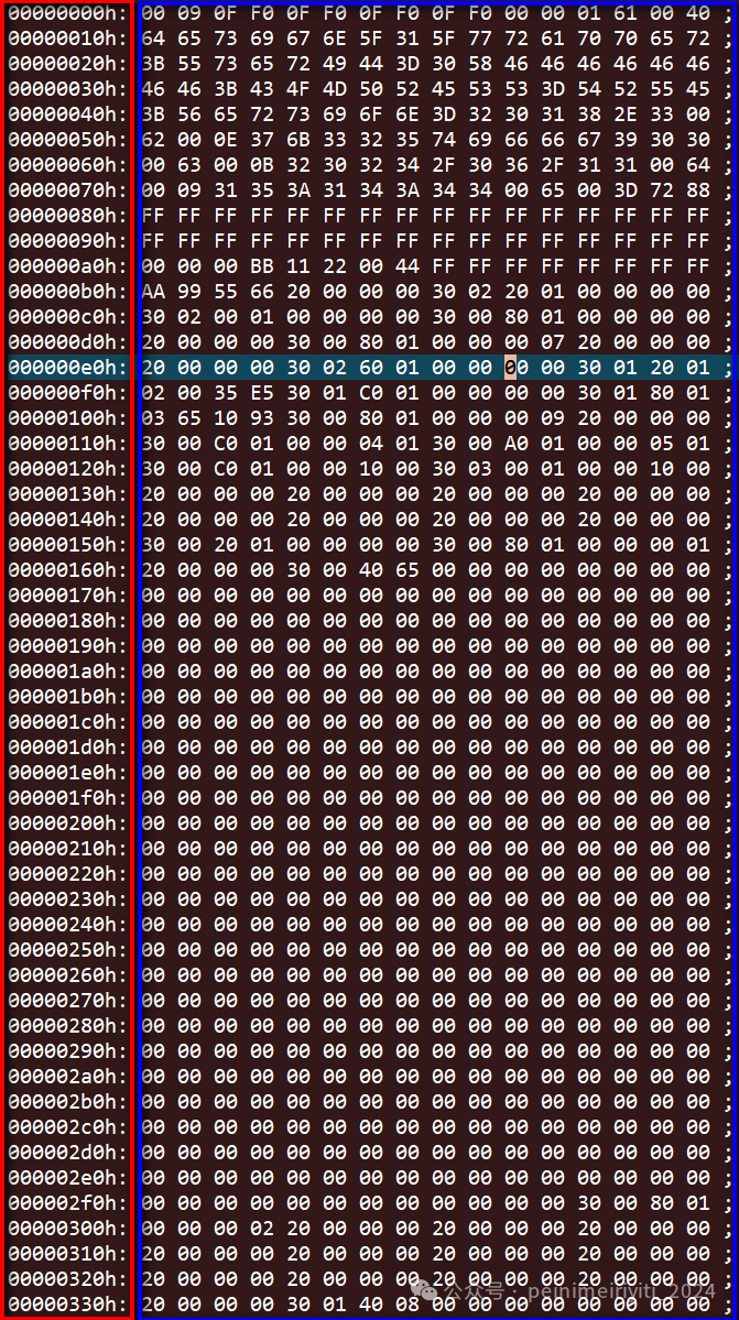 First, let’s take a look at the structure of this image:Blue box: DataRed box: Address (representing the address of the first byte after the semicolon), for example,The 0th number 00, its address is 00000000h,The 1st number 09, its address is 00000001h,The 2nd number 0f, its address is 00000002h,……The 16th number 64, its address is 00000010h,…….The 32nd number 3B, its address is 00000020h.Next, let’s look at what each byte represents.The first 112 bytes contain some basic information that is unrelated to your code, specifically:1) What tool generated this bitstream, for example, this bitstream was generated by Vivado 2018.3.2) What is the chip model, for example, this bitstream is for xc7a325t.3) The project name, for example, the name of this project isdesign_1_wrapper.4) The time the bitstream was generated, for example: this bitstream was generated on xx month xx day xx hour xx minute xx second of 2024.Starting from address 00000080h, let’s introduce what each data means.The data width is 4 bytes, for example, the address00000080h-00000083h should be viewed as a whole.The data in addresses 00000080h-00000083h is ff ff ff ff, which represents a 32-bit wide data.Eight such numbers are filled at the starting position.After the padding data, there is a data of 00 00 00 BB, followed by two data 11 22 00 44, which represent the bus width auto-detection word 1 and bus width auto-detection word 2, used to detect the data width during configuration. This means that during the configuration of the bitstream, the data is transmitted as 1 bit 1 bit, or 16 bits 16 bits, or 32 bits 32 bits.Then, there are two more data, ff ff ff ff and ff ff ff ff, which are also padding words.After that, there is a data of aa 99 55 66, which represents the synchronization word.As shown in the image below: starting from address 00 00 016c, this is the data stream generated by our logic code. Each number before this address has a specific meaning, which can be checked in the official manual.
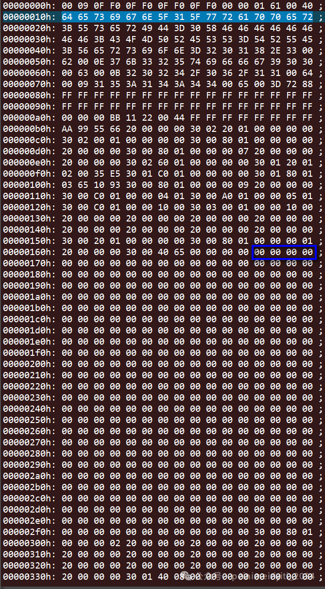 Here, I would like to share the official data manual, which contains a detailed introduction to the bitstream contents. You can refer to your own bitstream item by item.
File shared via cloud drive: ug470_7Series_Config.pdf
Link: https://pan.baidu.com/s/1wEZsBDxG_wmFqmMRMK7qYg?pwd=xdd1 Extraction code: xdd1