
Chiplet technology and NoC technology have become important methods to address the limitations of Moore’s Law. Modern CPU chips no longer use ordinary IO interfaces; instead, they utilize a standard NoC bus interface that can connect to dedicated NoC bus DIEs (tentatively referred to as IO DIEs) using Chiplet technology. By integrating multiple CPU cores or heterogeneous cores with multiple IO DIEs through Chiplet technology, larger-scale chips can be produced. The emergence of Chiplet technology and NoC technology has ushered in a golden age of architectural development, where heterogeneous computing and Domain-Specific Architecture (DSA) are gradually taking center stage, leading to various efficient architectures in the field of artificial intelligence. Even Nvidia’s latest Hopper GPU is beginning to align with DSA. One of the cores of heterogeneous computing is interconnectivity; traditional PCIe buses lack a cache coherence mechanism, resulting in poor memory performance and unacceptable latency. This has led to the emergence of protocols such as CCIX and CXL, which are built on PCIe but offer cache coherence support while maintaining PCIe compatibility. At this year’s FCCM conference, a paper related to CCIX was jointly published by TU Darmstadt and Reutlingen University, which uses CCIX as the interface between FPGA and Host and provides a detailed evaluation of the differences between CCIX and PCIe. We present the translation of this paper for readers’ enjoyment.

Abstract: For a long time, most discrete accelerators have used various generations of PCI-Express interfaces to connect to host systems. However, due to the lack of support for coherence between the accelerator and host caches, fine-grained interactions require frequent cache flushes and may even necessitate the use of inefficient non-cacheable memory regions. The Cache Coherent Interconnect for Accelerators (CCIX) is the first multi-vendor standard that supports cache-coherent host-accelerator attachments and has demonstrated the capabilities of upcoming standards such as Compute Express Link (CXL). In our work, we compared the usage of CCIX and PCIe when connecting an ARM-based host to two generations of FPGAs that support CCIX. We provided low-level throughput and latency measurements for access and address translation, and examined application-level use cases for fine-grained synchronization using CCIX in FPGA-accelerated database systems. We demonstrated that particularly small reads from FPGA to host can benefit from CCIX, as its latency is approximately 33% shorter than PCIe. However, the latency for small writes to the host is about 32% higher than PCIe due to the higher coherence overhead. For database use cases, even under high host-FPGA parallelism, CCIX can maintain constant synchronization latency.
01

Introduction
When combining traditional software-based processing on host CPUs with dedicated hardware accelerators to achieve higher performance or efficiency through heterogeneous computing, the nature of the interface between the host and the accelerator is a critical design decision.
For most discrete accelerators, such as GPU or FPGA boards, PCI Express (PCIe) has long been the primary interface. Its performance has steadily improved, with the latest widely deployed PCIe 4.0 version achieving 1.97 GB/s per lane. However, PCIe is primarily optimized for high-throughput bulk transfers. For example, as shown in [1], a transfer size of 128 to 256 KB is required to achieve at least 50% of the theoretical bandwidth. For the smaller transfer sizes required for fine-grained host-accelerator interactions (down to cache line size), achievable throughput significantly decreases. Although PCIe has added extensions such as Address Translation Services (ATS) and Page Request Interface (PRI) to support shared virtual memory or atomic operations, most implementations do not include cache coherence mechanisms.
This makes fine-grained interactions very costly, as cache flushes are required on either the host or accelerator side when synchronously executing or exchanging small parameters or results, or the memory regions used for data transfers must be marked as non-cacheable, slowing down access speeds for the processing elements (host or accelerator) at their physical locations.
To address this issue, many interfaces and protocols that cover cache coherence have been proposed. In this work, we investigate the use of Cache Coherent Interconnect for Accelerators (CCIX), which is the first interface designated as a multi-vendor standard and implemented across multiple different accelerator and host architectures. Once protocols like Compute Express Link (CXL), which have broader industry support, enter the market, further improvements are expected in the near future.
We provide detailed low-level measurements for various CCIX access scenarios, as well as application-level use cases. The latter involves running a database management system (DBMS) utilizing near-data processing (NDP) with FPGA accelerators and high-performance synchronization between the host and the accelerator. To our knowledge, this is the first use of a cache-coherent accelerator interface for this purpose.
We will outline some interfaces and protocols in the next section, then discuss CCIX details, especially regarding FPGA accelerators in Section III. However, our main contribution is the evaluation, which we present in Section IV, followed by low-level features in Section V, and application-level use cases in Section VI. We summarize and look forward to future work in Section VII.
02
Related Work
a) PCIe:PCI Express [2] is the standard for connecting peripherals to desktop and server systems. PCIe expands the bandwidth of a link by bundling multiple lanes for a single device. In version 1.0, it was capable of transferring at a rate of 250 MB/s per lane. Each subsequent version has roughly doubled the bandwidth, now reaching 7.88 GB/s per lane in version 6.0. Currently, version 6.0 has just been specified, while hardware for version 5.0 is about to be released, and version 4.0 is the most widely deployed version on current hardware. PCIe uses full-duplex serial links and employs a point-to-point topology, with two additional layers above the electrical link layer, namely the data link layer and transaction layer. These additional layers provide error correction and packet-based communication. In addition to basic operations such as data transfer and device initialization, PCIe also supports more advanced (optional) features such as PRI and ATS, but does not include cache coherence.
b) CCIX:CCIX [3], [4] is a high-level I/O interconnect that allows two or more devices to share data in a coherent manner. At the physical layer, it can be compatible with PCIe (although it may optionally allow higher signaling rates) and differs only in the protocol and endpoint controllers. It was introduced by the CCIX Consortium in 2016, which was founded by AMD, ARM, Huawei, IBM, Mellanox, Qualcomm, and Xilinx [5]. CCIX has been implemented on both ARM-based and x86-based CPUs.
c) Other Shared Virtual Memory (SVM) or Cache Coherent SVM Interconnects:CCIX is not the only competitor in the shared virtual memory interconnect space. Alibaba Group, Cisco Systems, Dell/EMC, Facebook, Google, HPE, Huawei, Intel, and Microsoft proposed CXL [6] in 2019 based on Intel’s previous work. While CCIX can run on older PCIe connections, CXL was initially designed based on PCIe 5.0. Therefore, CXL can achieve up to 32 GT/s (i.e., 3.94 GB/s) per lane and provides similar functionality to CCIX but uses a different logical view. CXL has seen broader industrial adoption than CCIX and is expected to become a major solution in the coming years.
Another option is the Coherent Accelerator Processor Interface (CAPI, later OpenCAPI) introduced by IBM in 2014. While the first version was also implemented on PCIe, more recent versions are vendor-specific interfaces. CAPI is primarily used for IBM POWER-based hosts, thus its scope is more limited than CCIX and CXL. In OpenCAPI 3.0 (x8 lanes), it provides 22 GB/s of bandwidth and read/write latencies of 298/80 ns [7].
While not directly extending PCIe like CCIX, another interconnect supporting cache coherence protocols is Gen-Z [8]. It offers speeds of up to 56 GT/s per lane and allows multiple lanes to be combined similarly to PCIe. Despite its promising features, Gen-Z hardware has not yet been commercially released, and the technology will be merged into CXL.
d) Database Acceleration on FPGA: [9] provides a good overview of using FPGAs to accelerate database operations. The most common approach, such as in state-of-the-art solutions like Centaur [10], uses FPGAs as offload accelerators for large-scale filtering, sorting, joining, or arithmetic computations. However, this operational mode incurs significant costs for data transfers from FPGA to FPGA, and differs from the near-data processing methods studied here that aim to avoid these transfers.
03
CCIX Architecture and Its Use on FPGA
This section will outline the general CCIX architecture and discuss its use in two different FPGA families.
A. Overall Overview
Devices connect to CCIX at the endpoint. For the discussion here, the relevant types of endpoints are Host Agents (HA) and Request Agents (RA). HA acts as the “owner” of physical memory, providing coherent access to physical memory, while RA performs non-local reads and writes to remote memory by communicating with the owning HA. The difference between CCIX and PCIe is that RA can provide its own cache but maintains coherence with HA through CCIX. On the HA side, changes in cache state will be propagated to the accessing RA by sending appropriate messages. CCIX itself accesses using physical addresses but can optionally use existing PCIe mechanisms to allow accelerators to use virtual addresses. To perform actual address translation, CCIX relies on the PCIe ATS mechanism, which is also one reason why CCIX-attached accelerators maintain traditional PCIe connections with the host on different PCIe virtual channels (VC). In various CCIX topologies, including mesh and switch hierarchies, we adopt a simple topology that relies on a direct connection between the host and the accelerator. Furthermore, since the hardware interface level supports all necessary operations, including address translation and coherence, no special device drivers or custom firmware are required on the host.
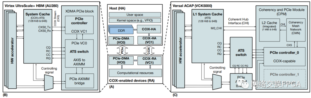
Figure 1 (A): Architecture of a host with CCIX capabilities acting as HA, with the attached CCIX accelerator acting as RA. Left (B): Implementation of CCIX-RA SoC on Xilinx UltraScale+ HBM devices. Right (C): Implementation of CCIX-RA SoC on Versal ACAP devices.
Figure 1-(A) shows the high-level architecture of a cache-coherent host FPGA attachment supporting CCIX. At the top of this block diagram is the host, and at the bottom is the accelerator, both connected via a PCIe interface that supports CCIX. CCIX uses multiple VCs on the PCIe transaction layer to transmit both PCIe and CCIX traffic over the same PCIe slot. In slots that support CCIX, the transaction layer uses VC0 for PCIe packets and VC1 for CCIX packets, sharing the same physical and link layers. However, CCIX can optionally use the Enhanced Speed Mode (ESM), which increases the signaling rate. For the PCIe 4.0 attachment we used, ESM increases the rate from 16 GT/s to 25 GT/s, transmitting 128 valid payload bits per transfer. If both parties (i.e., RA and HA) support it, ESM mode will be automatically enabled during the CCIX discovery phase at boot.
B. FPGA RA Using Xilinx XDMA
Xilinx Virtex UltraScale+ HBM devices support CCIX, but the CCIX functionality must be implemented as a reconfigurable “soft” logic in the form of an extended XDMA IP block. As shown in Figure 1-(B), key modules include a CCIX-capable PCIe controller, an ATS switch, and a PCIe-AXIMM bridge. The ATS switch is used to insert virtual-to-physical address translation requests into regular PCIe communication via PCIe VC0, and then retrieve their results. It also includes a small Address Translation Cache (ATC) to buffer existing translation results to avoid relatively expensive address translations for known mappings. The AXIMM bridge provides memory-mapped communication between the host and the accelerator (primarily control plane traffic). For data plane access, the accelerator employs an on-chip cache implemented using Xilinx’s system cache IP block [11], which interacts with the CCIX coherence mechanism using CCIX stream protocol. Misses in this cache become remote memory accesses, forwarded to HA via CCIX to retrieve data. In turn, HA ensures coherence between the FPGA-side SC and the host-side cache.
C. FPGA RA Using Xilinx CPM
The latest Xilinx Versal devices have optimized “enhanced” support for CCIX within their chips. Specifically, the Coherence and PCIe Module (CPM) IP block [12] includes an integrated L2 cache that communicates with a chip-wide coherence mesh network using ARM’s CHI protocol, which in turn interfaces with the CCIX-capable PCIe controller via CXS. As with the previous UltraScale+ devices, two PCIe VCs are used to separate PCIe and CCIX traffic running on the same PCIe slot. Our setup only requires one of the two CCIX-capable PCIe controllers provided by the CPM module. The ATS switch and AXIMM blocks are used as before.
D. Address Translation
When the system cache (SC) receives read/write requests from the accelerator, it checks the virtual-to-physical mappings in the ATC. If the SC does not find a valid translation in the ATC (i.e., ATC miss), it will request a translation from the host using the PCIe ATS functionality via VC0. The ATS interface on the system cache provides translation services through a request completion protocol [13] via four stream interfaces: incoming completer request (CQ), outgoing completer completion (CC), outgoing requester request (RQ), and incoming requester completion (RC). Replies from the host (e.g., reserved physical addresses) are passed back to the FPGA using the same mechanism.
E. CCIX Timing Model
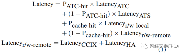
The average latency of CCIX transactions is shown in Formula 1. The latency of each transaction depends on the probability of having valid cached address translations available in the ATC versus the probability that ATS must request new translations from the host, as well as whether the requested data exists in the local on-chip cache. If it must be requested from a remote HA, please note that when using ESM, the physical CCIX latency may be shorter than the physical PCIe latency.
04
Experimental Setup and Evaluation
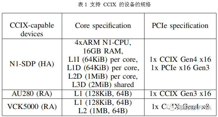
We conducted practical evaluations on real hardware, using the CCIX-capable ARM N1-SDP platform as the host and Xilinx’s Alveo U280 (AU280) and VCK5000 CCIX-attached boards with UltraScale+ HBM and Versal ACAP FPGAs as accelerators. Table I shows the specifications of the different devices.
A. Measurement Setup
All low-level benchmarks described later use the same basic measurement methodology, which consists of three main components: a software application programming interface (API), hardware modules, and the aforementioned on-chip CCIX components. The software API runs on the host, responsible for executing benchmarks and reading the CCIX latency characteristics analyzed by the hardware. The software API has four main tasks: a) allocate buffers in host memory, b) initialize hardware modules for access measurements, c) retrieve latency data recorded by hardware modules, and d) analyze results. The pseudocode for the software API is shown in Algorithm 1. Note that we randomize addresses to force SC misses, ensuring that the CCIX transfers of interest actually occur.
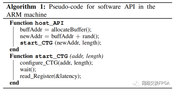
A hardware module called the CCIX Traffic Generator (CTG) uses a get/store method to capture CCIX latency. This module accepts requests from the software API in the host for startTrans calls (including type, virtual address, and length). After the API request, the CTG creates requests to the SC via the AXI4-MM interface, with the SC performing the role of CCIX RA, and then calculates the time it takes for the response to reach the SC. The captured timing can then be read via the software API. Note that we only consider a transaction complete once all its data has arrived.
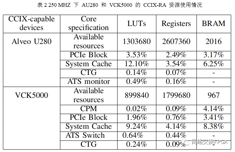
Table II shows the FPGA resources required for the simple CCIX-RA we examined. As shown in Figure 1-(C), the VCK5000 uses a PCIe controller in the form of a hardened CPM module, but still requires some additional “soft” logic to support PCIe transfers and ATS translations.
B. Low-Level Experimental Evaluation
Experiment 1: CCIX vs. PCIe – Latency and Throughput.
In this experiment, we compared the latency of CCIX and PCIe transfers for relatively small block sizes (32B to 16KiB) in fine-grained interactions (and much smaller than the bulk transfers examined in [1]). The open-source TaPaSCo [14] framework was used to test DMA transfers. In this experiment, we eliminated ATS latency by ensuring that address translations were already present in the ATC. Figures 2-(A) and 2-(B) show the read and write latencies for PCIe and CCIX traffic, respectively. For PCIe-DMA transfers, we used TaPaSCo’s high-performance DMA engine, directly using the physical addresses of the host memory data by setting different data transfer sizes. For CCIX measurements, a buffer was allocated in host memory, and its virtual address was passed to the CTG module.
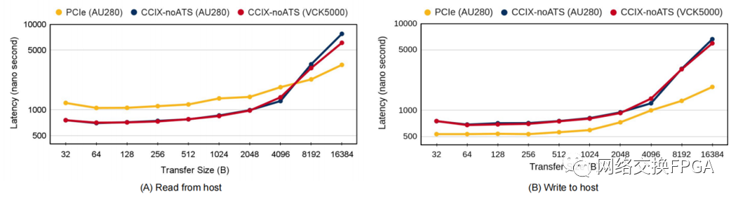
Figure 2 compares the read/write access latencies of CCIX and PCIe on AU280 and VCK5000.
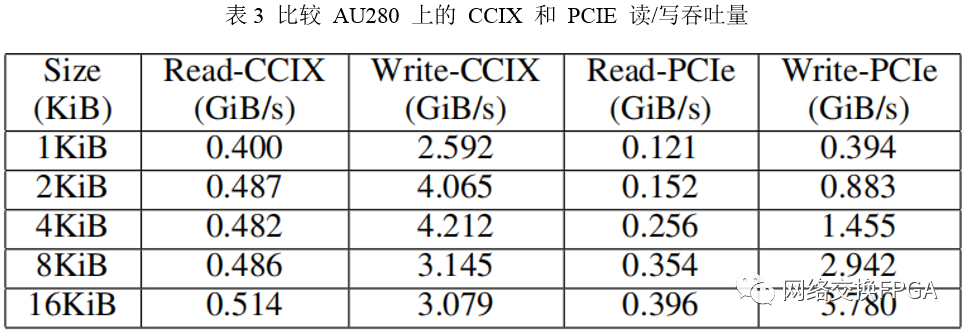
Our evaluation indicates that on both AU280 and VCK5000, CCIX transfers exhibit better host read latencies compared to PCIe-DMA transfers, as long as the transferred data is shorter than 4 KiB. In both cases, the acceleration is due to the optimized packet protocol used by CCIX. However, when using the optimized packet protocol to write from FPGA to host memory, CCIX incurs longer latencies than PCIe transfers, as these writes involve the coherence mechanism. Our throughput measurements show that for data set sizes of 1KiB, 16KiB, and 32KiB, CCIX’s read throughput relative to PCIe is 3.3x, 1.29x, and 0.87x, respectively. Other data points for read and write throughput are shown in Table III.
Experiment 2: Cost of ATS.
The ability to transparently resolve virtual addresses greatly simplifies accelerator design and host interfaces. However, this operation can be costly, as it may trigger slow full page table traversals on the host if the requested translation is not present in one of the host’s IOMMU TLBs. In Experiment 1, we examined accesses that did not require address translation (no ATS). However, to examine the cost of ATS, we now constructed two access scenarios, as shown in Figure 3: in the first scenario (using ATS), we forced misses in both SC and ATC, thus always incurring ATS overhead. In the second (no ATS), we allowed ATC hits but still forced SC misses to ensure that actual CCIX transactions occurred. The results indicate that particularly for smaller transfers, ATS overhead can be significant, leading to a threefold increase in access latency when ATC misses occur. However, for transfers of 32KB and above, transfer time begins to dominate ATS overhead.
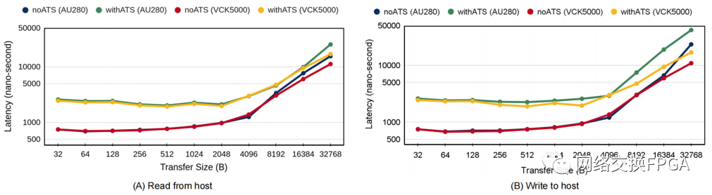
Figure 3 shows the impact of ATS on CCIX access latencies for random accesses to the RA module from Alveo U280 and VCK5000 cards.
To further investigate ATS latency, we can leverage the fact that the entire ATS mechanism is implemented in the ATS Switch block of the SoC. Therefore, we can monitor the request/reply interface of this module to capture the exact request-response times of ATS operations themselves. Figure 4 shows the CCIX access latencies for 64 B (cache line size), 128 B, and 4 KiB blocks. Since the Linux Page Size is 4KiB, these requests each require only one ATS translation. As the request size increases, more translations are needed. The initial access to the buffer allocated in host memory has the longest latency. Subsequent sequential accesses have less ATS overhead, even when crossing to another page at 4 KiB. We assume this is due to the host IOMMU performing pre-translation for the sequential accesses used here. For the case of repeated 64 B reads, by comparing the latency required for the host IOMMU to respond to ATS requests (≈ 617 ns, captured at the ATS switch) with the known latency of reading 64B in the case of SC misses (≈ 700 ns, from Figure 3-(A)), the ATC itself seems to require (2453 – 617 – 700 ≈ 1136 ns) to operate.
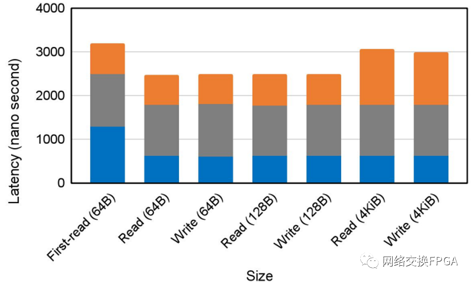
Figure 4 compares the read/write latencies of CCIX-RA on Alveo U280 and ATS latencies.
One way to improve CCIX traffic latency is to mitigate the impact of address translation. This can be achieved by utilizing Linux large page support. This will result in larger pages, thereby requiring fewer new translations when crossing page boundaries. The N1-SDP platform indeed supports different sizes (i.e., 64KB, 2MB, 32MB, and 1GB) of huge pages at boot. We adopted this approach in the database use case (Section V) to enhance performance.
Experiment 3: Data Locality.
The use of CCIX allows accelerators to use their own caches, confident that they will always remain coherent with the host. To demonstrate the best-case baseline performance of the two SoCs, we evaluated the case where all accesses hit in the device’s cache, referred to as local data in Figure 5, and measured the latencies of these hits. For comparison, we also show the remote case of cache misses. The simpler cache hierarchy in AU280 achieves smaller latencies (write ≈ 80 ns, read ≈ 100 ns) for smaller transfer sizes compared to the two-level cache (write ≈ 150 ns, read ≈ 170 ns) on VCK5000. However, for larger transfers, the two-level hierarchy becomes faster.
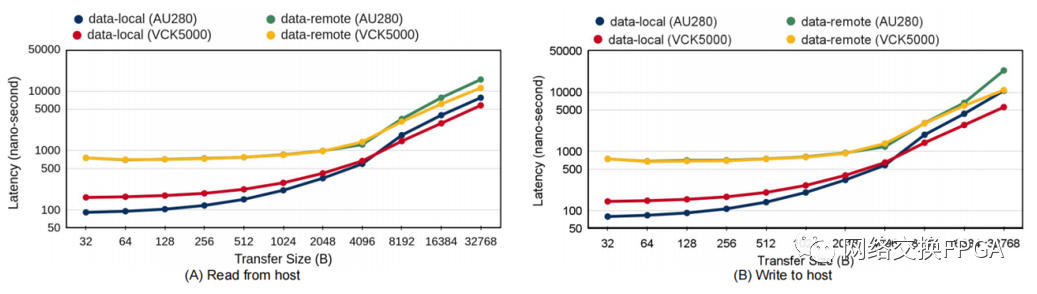
Figure 5 shows the impact of data locality on CCIX latencies for AU280 and VCK5000.
Experiment 4: Coherence Efforts.
In this case, an application on the host allocates a shared buffer that both the host and the accelerator access and modify concurrently. These concurrent accesses/modifications increase coherence work, thereby increasing access latency. Large pages are used to avoid ATS overhead. As described in Algorithm 2, the hardware CTG and software API simultaneously modify cache lines in the shared buffer. Initially, we measured using a 2 MiB buffer, then reduced it to 512 KiB, 128 KiB, and 32 KiB to increase contention, thereby increasing the effort required to maintain coherence. This reduction in buffer size is shown on the left Y-axis of Figure 6. For each of these shared buffer sizes, we performed 1024 accesses to random addresses in the buffer using a single CPU core and FPGA from two hosts, tracking their latencies. As expected, both contention increases with the number of accesses and the reduction in buffer size. In both cases, the likelihood of coherence conflicts that must be resolved increases. Interestingly, the additional coherence work primarily affects host accesses, while the FPGA-side access latencies remain almost unchanged. This is examined in more detail on the right side of Figure 6, which plots the access times as a histogram, now for 20,000 accesses, for the 32 KiB and 2 MiB shared buffer sizes. While the times are longer, the remote accesses from the FPGA side exhibit much less “jitter” (narrower distribution) than local host-side accesses. Note that the very short outliers for FPGA-side accesses are actually hits in the SC, which are more likely in the smaller 32 KiB than in the larger shared buffer. In this experiment, only one core on the host accesses the shared buffer. To further investigate, we used multiple cores on the host to modify and access the shared buffer. Our evaluation indicates that increasing the number of cores from 1 to 3 in the 32 KiB address range actually reduced the average access latency from the local host side from 333 ns to 235 ns due to more cache hits. On the other hand, due to more cache misses, the device access latency increased from 674 ns to 741 ns. For larger memory ranges, access times remained almost constant.
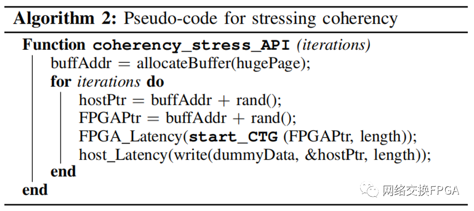
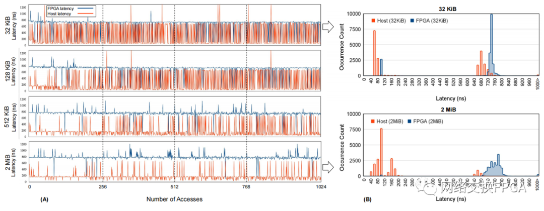
Figure 6 shows the coherence work of increasing host-FPGA access contention with a single CPU core. Left (A): Simultaneous 1024 random accesses within the address range from 2 MiB to 32 KiB. Right (B): Histogram showing access latency “jitter” for the two address ranges.
Experiment 5: Atomic Operations.
CCIX also enables atomic transactions between RA (e.g., AU280) and HA (e.g., N1-SDP) by supporting AtomicStore, AtomicLoad, AtomicSwap, and AtomicCompare operations. They are constructed as multi-step sequences of AXI4-MM requests on the RA side. Our evaluation indicates that AtomicCompare initiated from the host requires 50 ns, while AtomicCompare initiated from the accelerator requires 740-800 ns.
05
Database Applications
After these detailed low-level measurements, we now examine the application-level use of CCIX in scenarios requiring fine-grained host-accelerator interactions. As a realistic scenario, we choose the field of database acceleration. The system under study is neoDBMS (Figure 7) [15], [16], a PostgreSQL-based DBMS that uses FPGA-accelerated NDP. In this way, computation is moved closer to storage (e.g., flash, NVM), assuming that storage is directly connected to the accelerator. Using NDP reduces data transfers and improves overall system performance. However, NDP in database applications faces some challenges, such as synchronization and transaction consistency. In databases, there are two types of transactions in NDP mode: read-only NDP and update NDP. In read-only NDP, each transaction operates on its own snapshot to avoid interference. This requires first collecting all DBMS updates in the host’s main memory and then transferring the changed DBMS state to the accelerator during each NDP call [15].
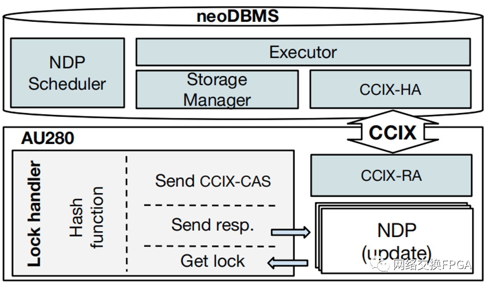
Figure 7 Architecture of neoDBMS with shared lock table
In update NDP, it is challenging to keep transactions free from interference due to concurrent modifications by both the host and the accelerator on the same record. Initially, the same current version of the record exists in both the accelerator and the DBMS memory. If both create new successor versions of the record simultaneously, it leads to two current versions branching, resulting in an unresolved inconsistency known as a write/write conflict. One way to mitigate this inconsistency is to exclusively lock the entire database table before execution, but this severely limits concurrency. Another approach is to use a fine-grained cache coherence shared lock table that supports record-level locking, allowing the version of each record to be locked to synchronize modifications between the DBMS and the accelerator.
A. Shared Lock Table
To achieve consistent and interference-free update NDP operations between the DBMS and the accelerator, low-latency cache coherence invalidation and synchronization mechanisms are required. To address the write/write conflicts in the aforementioned neoDBMS, we implement a shared lock table using a CCIX-based solution. Without CCIX, the cost of synchronization would be much higher and likely waste any performance gains achieved through NDP processing. To this end, our modified neoDBMS allocates a shared lock table in the host memory, where both the host and FPGA request to lock records before updating them. neoDBMS relies on the support of large pages (i.e., HugeTLB Page) in the Linux kernel to request physically contiguous memory pages for allocating the lock table and ensuring they are pinned. Since the size of the lock table is relatively small and entries are accessed very frequently throughout the runtime of the DBMS, pinning the table in physical host memory is effective.
Row-level locks are executed by inserting an entry into a queue located in a hash bucket. Thus, the queue can simultaneously contain multiple lock entries. The bucket position is calculated by applying a hash function to the record version identifier. Figure 8 shows an example of two concurrent processes, one on the host and one on the device, requesting locks for the same record version (i.e., Rv2). Applying the hash function to the record version identifier causes both processes to attempt to insert locks into the same lock queue located in the same hash bucket, numbered 2 here. In this example, first, the device requests the lock and immediately acquires it. The first slot represents the process currently holding the lock and allowed to modify the data. Later, the host attempts to request the same lock. Since the first slot of the lock queue is already occupied, the host cannot acquire the lock and appends its request to the end of the lock queue, waiting. Once the device is done, it releases the lock by moving the entire queue to the left, granting the lock to the next process now located at the head of the queue. The host then acquires the lock and can continue execution.
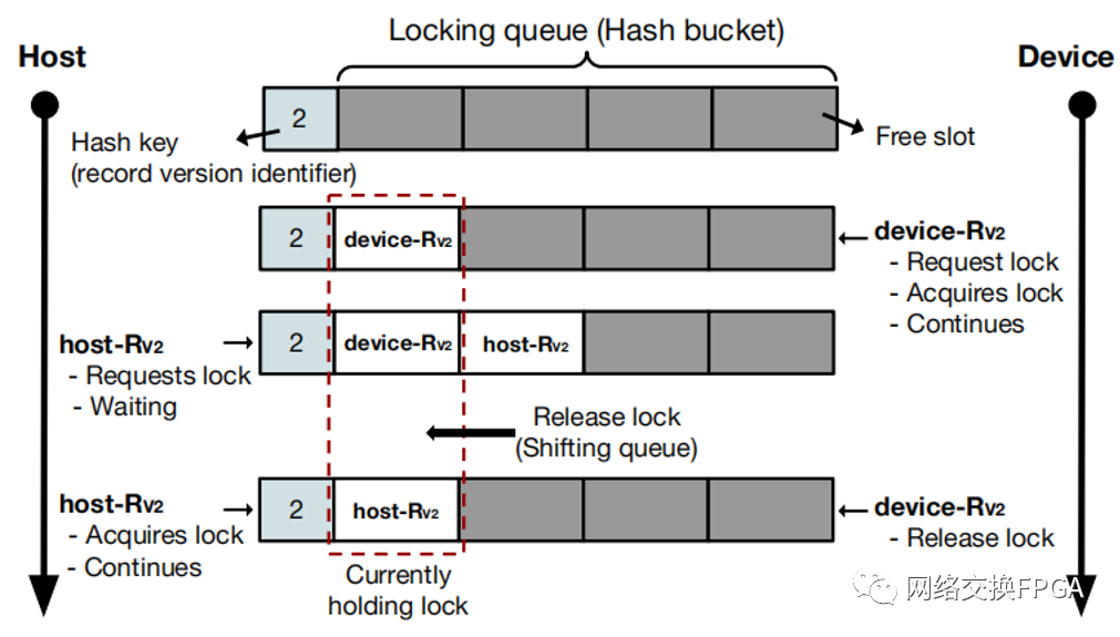
Figure 8 Example of a single hash bucket in the shared lock table, where concurrent lock requests from the host and device queue for the same record version.
On the FPGA, a Bluespec module has been developed to handle lock requests from the NDP-update module. This module creates a hash table organized lock table on the provided virtual address. The allocated buffer address and lock table are specified by neoDBMS. The module receives/sends lock requests/responses via stream interfaces. Upon receiving a lock request, the module creates a CCIX atomic compare and swap (CAS) operation to place the lock and update the queue, which is then sent to the host by the CCIX-RA on AU280. Through the cache coherence shared lock table and the adopted CCIX atomic operations, we achieve fine-grained collaborative processing of data between the DBMS and FPGA.
B. Evaluation
To evaluate the performance of the CCIX-based synchronization mechanism, we measured the end-to-end lock request latencies of neoDBMS running on the N1-SDP platform and the AU280-based accelerator, as shown in Figure 9. Since the size of the shared lock table exceeds the Linux 4KiB page, accesses risk incurring longer ATS overhead. This has been avoided by using large pages. The hardware module performs a request independent of the actual shared lock operation to “preheat” the ATC by performing physical translations of the large pages. Then, all actual lock requests will have ATC hits and will not be affected by ATS overhead.
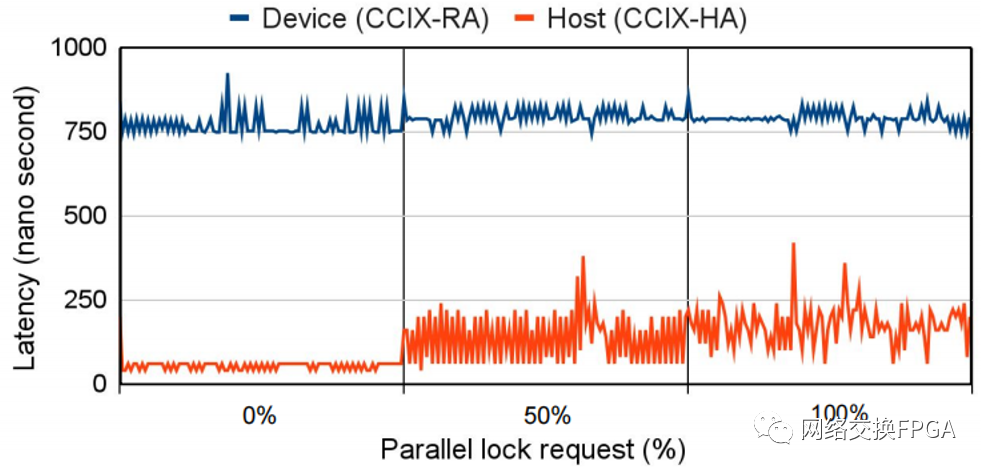
Figure 9 Impact of parallel access to the shared lock table
In the experiment, both neoDBMS (on a single CPU core) and the accelerator continuously create lock requests, while we increase contention on the other side. Under low contention, neoDBMS is able to lock record versions in the locally resident lock table within 80 ns. Under high contention, the local locking latency of neoDBMS increases to 200-250 ns. Locking from the accelerator, of course, takes longer since remote accesses are performed on host memory, but the observed latencies of 750 to 800 ns are typical latencies for CCIX atomic CAS operations (see Experiment 5 above), and importantly, are not affected by increased contention. While this confirms the behavior already observed in Experiment 4, it is interesting to note that it applies not only to the simple read/write operations of Experiment 4 but also to the more complex atomic CAS accesses used here.
06
Conclusion
We investigated the use of CCIX for fine-grained interactions between hosts and FPGA-based accelerators. In our results, we demonstrated that especially for smaller transfer block sizes, shorter latencies can be achieved compared to PCIe. Furthermore, the transparent integration of address translation with CCIX operations supports a cache-coherent shared virtual memory (ccSVM) programming model between hosts and FPGA accelerators, which has traditionally only been applicable to highly specialized platforms such as Convey HC-level machines. For database use cases, it is evident that while CCIX remote accesses are slower than local accesses, even higher degrees of contention access to shared data structures such as lock tables are not adversely affected.
Our results also indicate that there is optimization potential at multiple levels of the hardware/software protocol stack. For example, we have demonstrated the use of large pages to reduce address translation overhead. More efficient application-specific translation mechanisms could also be inserted into the SoC, as all translations occur in the ATS Switch module, which has well-documented interfaces that could be replaced with custom versions. This could be leveraged, for example, in the DBMS use case in Section V, where even for random access patterns exceeding ATC capacity, ATS could be completely avoided. The ATC itself also seems to have optimization potential, but this would require greater engineering effort as it is more tightly integrated with the vendor-provided system black box.

THE END
Disclaimer:This article is reproduced from the FPGA public account of network delivery. If there are any issues regarding the content, copyright, and other matters, please contact the staff via WeChat (13237418207), and we will connect with you to delete and handle it as soon as possible!Submissions/Recruitment/Advertising/Course Cooperation/Resource Exchange, please add WeChat: 13237418207
Previous Recommendations
FPGA Digital Signal Processing Communication Class I/Q Signal and Generation
What is the difference between solder mask and solder mask layers in PCB? A detailed explanation with illustrations!
“180-Day FPGA Development Online Practical Training Class – Fanyi”
Considerations for FPGA and High-Speed ADC LVDS Data Interface Design

Scan the code to add customer service WeChat to note “ Enter the group“ to pull you into Fanyi Education Official Technical WeChat group to communicate technical questions and insights~
Share and like on WeChat ❤️ “ Three links support!