Today, the high integration and miniaturization of electronic products make chips prone to overheating, which has become an “invisible killer” for electronic devices. At the same time, chips face severe heat dissipation challenges: as the chip manufacturing process becomes more refined, the heat flux density increases, leading to higher thermal design power and more significant constraints on chip performance. Efficient thermal management has become a bottleneck restricting the release of chip performance.
Recently, the research team from the Ningbo Institute of Materials Technology and Engineering, Chinese Academy of Sciences (hereinafter referred to as “Ningbo Materials Institute”), successfully prepared a 4-inch ultra-thin, ultra-flat diamond self-supporting film, marking an important step in overcoming the long-standing warping problem that restricts chip bonding processes and promoting the development of diamond in the field of chip thermal management.
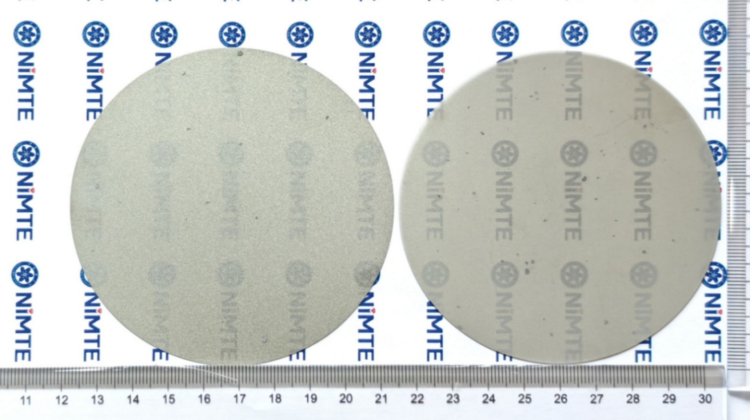 ▲ Photograph of low-warp ultra-flat diamond self-supporting film (front view)
01
Diamond Heat Dissipation
The Real Bottleneck of Ideal Materials
During operation, when the heat generated internally by the chip cannot be effectively dissipated, localized areas can form “hot spots,” leading to decreased chip performance and even hardware damage. More than half of device failures are directly related to overheating.
Especially for third-generation semiconductor chips such as silicon carbide and gallium nitride, when they operate under high-frequency and high-power conditions, they generate high heat flux densities, making traditional heat dissipation solutions that rely on reducing the shell-environment thermal resistance increasingly untenable.
Diamond is a natural “heat dissipation champion”—its thermal conductivity exceeds 2000W/m·K, more than five times that of copper.
If the chip is directly “bonded” to a diamond substrate, it can significantly reduce the “thermal resistance near the junction” (the resistance to heat transfer between the chip’s heat-generating core and the heat dissipation material) and the “junction temperature” (the temperature of the most critical heat-generating point inside the chip), akin to applying a “superconducting ice pack” to the chip core. This is also seen as an ideal solution for thermal management in future high-performance chips and 3D packaging.
However, diamond films are grown on other substrates, and the intrinsic thermal expansion coefficient differences between diamond and the substrate, along with issues related to nucleation and growth process compatibility, lead to severe warping of the diamond film after detaching from the substrate, failing to meet the stringent requirements for ultra-flatness in chip bonding processes.
This has kept the thermal potential of diamond “sealed.” Solving the substrate warping issue is key to applying diamond films in chip bonding.
02
Process Innovation and Breakthroughs
Opening Up the Channel for Diamond Chip Bonding Processes
The research team at Ningbo Materials Institute, based on self-designed and developed 915MHz-75kW microwave plasma chemical vapor deposition (MPCVD) equipment, has successfully prepared a 4-inch diamond self-supporting film with a thickness of less than 100μm through technological innovation and process optimization.
In a self-supporting state, the warpage can be stably controlled within 10μm, which is an order of magnitude lower than that of diamond films produced by conventional processes.
Most importantly, this ultra-low warpage endows the diamond film with extraordinary flatness, allowing it to spontaneously adhere to glass substrates without external force, exhibiting a unique “self-adhesion” phenomenon.
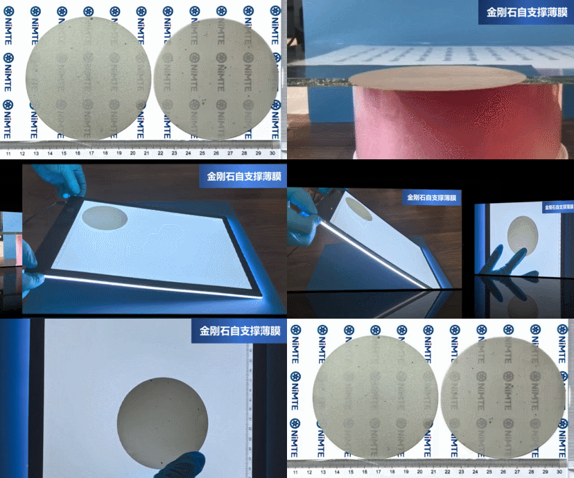
The ultra-thin self-supporting structure brings greater flexibility and multidimensional design freedom to packaging design, showcasing enormous application potential in advanced packaging processes such as heterogeneous integration and 3D stacking of semiconductor chips.
Currently, the research team is striving to develop ultra-thin, ultra-low stress diamond thermal conductive materials larger than 6 inches, continuously advancing and expanding their application in thermal management for high-power chips in AI, RF, and other fields.
Source:Ningbo Institute of Materials Technology and Engineering, Chinese Academy of Sciences
Editor: Song Tongzhou
