With the rapid development of the PCB industry, PCBs are gradually moving towards high-precision fine lines, small apertures, and high aspect ratios (6:1-10:1). The copper requirement for holes is 20-25μm, and for boards with a D/F line spacing of ≤4 mil, most PCB manufacturers face plating adhesion issues. Adhesion can cause direct short circuits, affecting the first pass yield during AOI inspection, and severe adhesion or excessive points that cannot be repaired can lead to scrapping.
Illustration of Plating Adhesion Issues: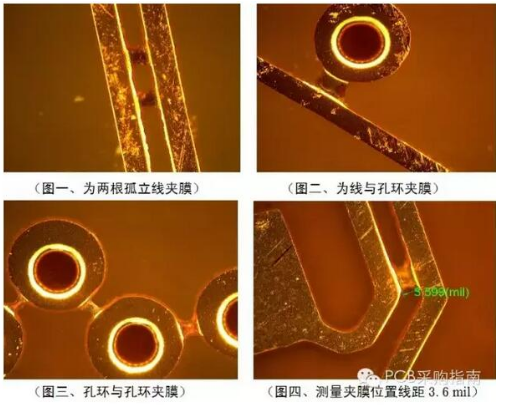 Analysis of PCB Plating Adhesion Principles① The copper thickness of the patterned electroplated lines exceeds the thickness of the dry film, which can cause adhesion. (Typically, the dry film thickness used by PCB manufacturers is 1.4 mil)② The combined thickness of the copper and tin on the patterned electroplated lines exceeds the thickness of the dry film, which may also cause adhesion.Analysis of Causes of PCB Plating Adhesion
1. Images and Photos of Boards Prone to Adhesion
 From the photos of the actual boards in Figures 3 and 4, it can be seen that the lines are relatively dense, and the aspect ratio of the engineering design layout is significantly different, which is not conducive to current distribution. The minimum D/F line gap is 2.8 mil (0.070mm), the minimum hole size is 0.25mm, and the board thickness is 2.0mm, with an aspect ratio of 8:1. This is considered a high-difficulty process board.2. Analysis of Adhesion Causes① High current density in patterned electroplating leads to excessive copper deposition.② The edges of the flying bar are not clamped, leading to thick plating in high current areas.③ The transformer failure results in a current setting larger than the actual production board.④ The C/S and S/S sides are reversed.⑤ The spacing is too small; boards with a spacing of 2.5-3.5 mil are prone to adhesion.⑥ Uneven current distribution due to the anode not being cleaned for a long time in the copper plating tank.⑦ Incorrect current settings (wrong model or incorrect board area input).⑧ Equipment failure causing PCB boards to remain in the copper tank for too long.⑨ Unreasonable engineering layout design, incorrect effective electroplating area provided by engineering, etc.⑩ PCB line gaps are too small, and special line patterns on high-difficulty boards are prone to adhesion.
Effective Improvement Solutions for Adhesion
1. Reduce the current density in the patterned electroplating and appropriately extend the copper plating time.
2. Increase the thickness of the copper plating on the board while appropriately reducing the current density of the patterned electroplating, thereby reducing the thickness of the copper plating on the pattern.
3. Change the bottom copper thickness from 0.5OZ to 1/3OZ. Increase the copper thickness on the board by about 10μm, reduce the current density in the patterned electroplating, and decrease the thickness of the copper plating on the pattern.
4. For boards with a spacing of <4 mil, procure 1.8-2.0 mil dry film for trial production.
5. Other solutions such as redesigning the layout, modifying compensation, adjusting line gaps, and reducing hole rings and pads can also relatively reduce the occurrence of adhesion.
Control Methods for Electroplating Production of Boards Prone to Adhesion with Small Line Gaps
1. FA: First, test a flying bar board with edge clamps at both ends. After ensuring the copper thickness, line width/spacing, and impedance are qualified, etch the flying bar board and pass the AOI inspection. If adhesion is found, immediately adjust the current and retest FA.
2. Stripping: For boards with D/F line gaps <4 mil, slow down the etching and stripping speed appropriately.
3. FA Personnel Skills: When the current indication for boards prone to adhesion is present, pay attention to evaluating the current density. For general boards with a minimum line gap <3.5 mil (0.088mm), control the current density of the patterned electroplating copper at ≦12 ASF to avoid adhesion. Except for particularly high-difficulty line patterns as shown below:
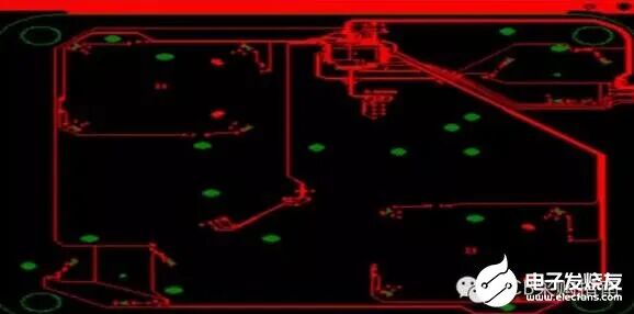
This patterned board has a minimum D/F line gap of 2.5 mil (0.063mm). Even under good uniformity conditions in the electroplating line of general manufacturers, it is still difficult to avoid adhesion. It is recommended to use ≦10 ASF current density for FA testing.
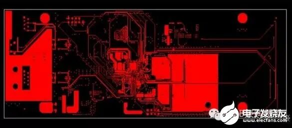 This patterned board has a minimum D/F line gap of 2.5 mil (0.063mm), with many independent lines and uneven distribution. Even under good uniformity conditions in the electroplating line of general manufacturers, it is still difficult to avoid adhesion. The current density for copper plating in patterned electroplating was 14.5 ASF for 65 minutes, resulting in adhesion. It is recommended to use ≦11 ASF current density for FA testing.Personal Insights and SummaryBased on my years of experience in PCB processing, almost every PCB factory faces adhesion issues when producing boards with small line widths and gaps, with the difference being the varying proportions of adhesion defects among different companies. The analysis is as follows:1. Each company’s PCB structure type is different, leading to varying difficulties in PCB manufacturing processes.2. Each company’s management models and operational methods differ.3. From my years of accumulated experience, for boards with small gaps, it is crucial to use only low current densities and appropriately extend the copper plating time. The current indication should be evaluated based on experience to determine the appropriate current density and copper plating time, paying attention to the clamping method and operational procedures. For boards with a minimum line spacing ≤4 mil, the flying bar board must pass AOI inspection for adhesion issues, which serves both quality control and preventive measures, thus significantly reducing the likelihood of adhesion during mass production.I believe that ensuring PCB quality requires not only experience and skills but also effective methods. Additionally, it depends on the execution strength of the production department personnel.Patterned electroplating differs from whole board electroplating, primarily in that it involves electroplating various models of board line patterns. Some boards have uneven line distributions, in addition to fine line widths and spacings, there are sparse lines, isolated lines, and various special line patterns. Therefore, I prefer to use FA (current indication) skills to address or prevent thick plating adhesion issues. Small adjustments yield quick results, and the preventive effects are significant.Disclaimer:This article is copyrighted by the original author and does not represent the views of the association.The articles promoted by the “Jiangxi Province Electronic Circuit Industry Association” are for sharing purposes only and do not represent the stance of this account. If there are any copyright issues, please contact us for removal.