Last year, I assembled an amplifier board using two LM1875 chips for ceiling speakers in my shop, which has been in use ever since.
Recently, I found a BBE sound exciter board online, which is said to enhance high-frequency details and improve low-frequency performance. However, since this BBE exciter board has its own bass and treble control circuit, installing it before the original amplifier board’s bass and treble control could easily muddy the music details and prevent the BBE board from performing at its best.
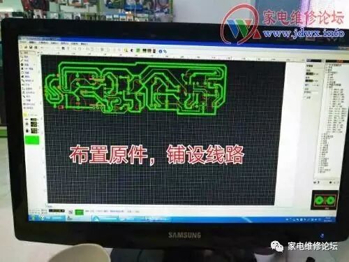
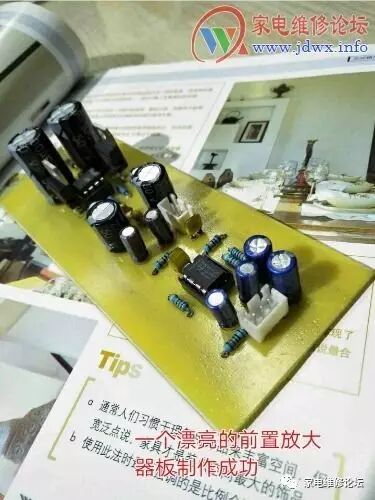
Therefore, I removed the original bass and treble control circuit and connected the BBE exciter board directly to the LM1875. After connecting the circuit and powering it on for a test, I first noticed that the vocals became clearer, and the sibilance was more pronounced. After listening to a few love songs sung by Jiang Zhiming and Zhou Hong, the sound was indeed very pleasant. However, even at maximum volume, it still felt insufficiently loud. When I tried increasing the volume on the computer, distortion occurred, indicating that the input signal to the BBE exciter board should not be too strong, or else it would distort. To achieve the desired volume, I would need to add an additional amplification circuit after the BBE board. After searching on Baidu, I finally chose a 5x preamplifier circuit based on the NE5532. Not only did the internet provide the schematic, but it also included a PCB layout. However, the resolution of the PCB layout was too low to use directly, so I thought of a PCB design software called Sprint-Layout 5.0, which could reference the PCB routing layout provided by Baidu, saving a lot of time in the process. So I got to work!


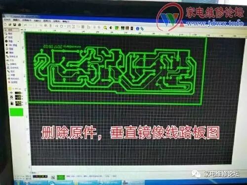
First, I downloaded and installed the Chinese version of Sprint-Layout 5.0. The specific usage is quite simple; the left side is the toolbar, and you can complete the wiring operation by directly clicking the corresponding tool with the mouse. The right side is the component library, where you can select components and drag them to the appropriate position to complete the component arrangement. I won’t go into detail about the specific steps here.

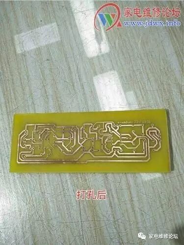
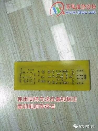
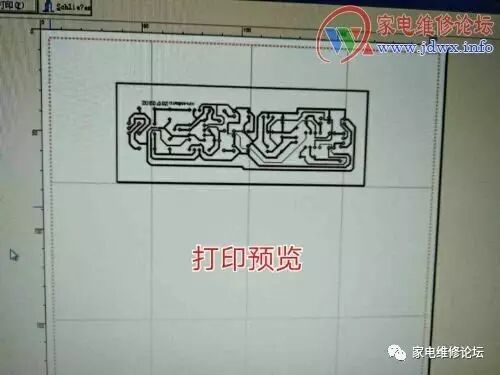
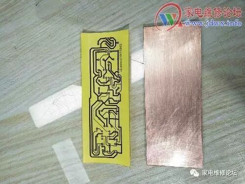
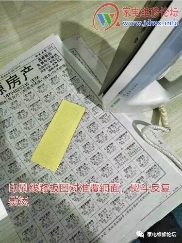
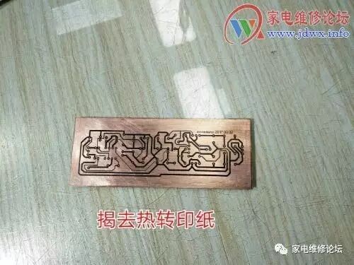
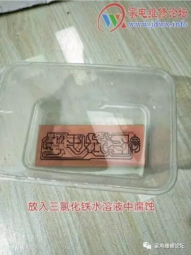
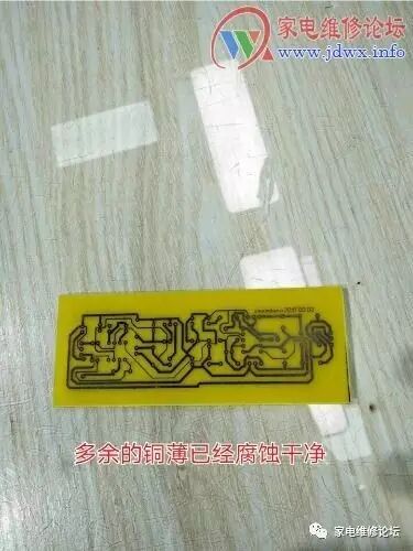
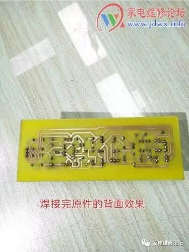
After completing the PCB design, I first placed special A4 heat transfer paper into the laser printer, then clicked “File–Print”. A beautiful PCB layout printed out. I cut out the printed layout, flipped it onto the prepared copper-clad board, and used an iron to repeatedly press and iron it. After removing the heat transfer paper, the printed layout was transferred onto the copper-clad board. I then placed it into a ferric chloride solution, shaking it continuously, and the excess copper was gradually corroded away. After a few minutes, I took it out and rinsed it with tap water, and a beautiful PCB board was ready. Finally, I polished, drilled, inserted components, and soldered everything in one go! How does it look? With such a beautiful and neat circuit board, don’t you feel an urge to try it yourself?
Original text: http://www.jdwx.info/thread-688000-1-1.html

Home Appliance Repair Forumjdwxinfo
▲ Long press to recognize the QR code to follow
Home Appliance Repair Technology Forumjdwx-cn
▲ Long press to recognize the QR code to follow