With the continuous development of process nodes (now commonly at 28nm, 22nm, 16nm, 14nm, and even some at 7nm), the performance demands of chips are increasing, and their scale is growing larger. Digital IC design engineers are becoming increasingly concerned about chip power consumption, especially for consumer electronic products on mobile devices, where power consumption requirements are particularly high. If the power consumption is too great, the entire product may just become a hand warmer, and the performance of the entire chip may be significantly compromised, failing to meet actual application needs. Today, I will guide you to review the definition of power consumption and its components, and summarize several commonly used methods for reducing power consumption.
Chip power consumption is divided into two main parts: dynamic power consumption and static power consumption.
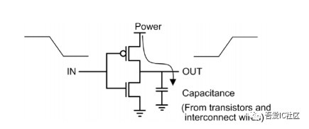
Figure 1: Dynamic Power Consumption Diagram
Dynamic power consumption is the energy consumed by the circuit when it is working (during transitions). For CMOS circuits, it is further divided into switching power consumption and short-circuit power consumption. Switching power consumption is the power consumed when charging the load capacitance during circuit transitions, while short-circuit power consumption is the power formed by the instantaneous current when both PMOS and NMOS are turned on during input transitions. It can be described by the formula:
Pdyn = (CL * Vdd² * Ptran * F) + (ttran * Vdd * Ipeak * F)
Where CL is the total load capacitance of the circuit; Vdd is the operating voltage; Ptran is the proportion of the working circuit; F is the operating clock frequency; ttran is the time when PMOS and NMOS are both conducting; Ipeak is the short-circuit current.
The first part of the formula represents switching power consumption, while the second part represents short-circuit power consumption. Generally speaking, as long as the gate’s slew rate is small enough, meaning ttran is fast enough, short-circuit power consumption can usually be ignored.
From the formula, we can see that the approach to reducing dynamic power consumption can be designed from aspects such as Vdd, F, CL, and reducing the number of gate transitions.
Now let’s talk about static power consumption. Static power consumption is the power consumed by leakage current in transistors when there are no transitions. It can be divided into the following four parts based on importance:
1. Subthreshold leakage current Isub: The current flowing from Drain to Source through the weak inversion layer.
2. Gate current Igate: The current flowing from the Gate to the Substrate due to tunneling and hot carrier effects.
3. Drain-induced gate leakage current IGIDL: The current flowing from Drain to Substrate induced by the strong electric field at the Drain terminal.
4. Reverse-biased junction current Irev: The current flowing from Drain and Source to Substrate formed by minority carrier drift and electron-hole pair generation in the depletion region.
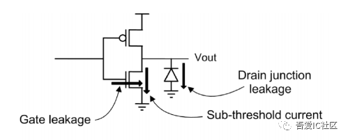
Figure 2: Leakage Current Diagram
So, what are the common methods to reduce power consumption in digital IC design? I have summarized a few methods as follows:
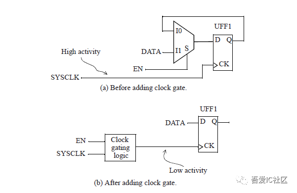
1. Clock Gating Technology. As we all know, in digital IC design, the transition rate of clock signals is relatively high, and thus the power consumption of clock signals accounts for about 20-30% of the total chip power consumption. The traditional design method keeps the clock signal always active (always on). Clock gating technology temporarily disables the clock signals of modules that are not in use through a control signal, thereby reducing the transition rate of the clock signal for that module and thus lowering the chip’s power consumption. There are many forms of clock gating, including root-level gating that is instantiated at the RTL level, as well as those added automatically by synthesis tools. From the perspective of digital front-end design, it is better to keep clock gating as close to the root as possible (because one gating can control more registers or clock units). Once a certain gating is turned off, it can save a significant amount of power consumption. Therefore, during the digital back-end implementation process, it is often encountered that the setup time for the gating enable pin E is difficult to meet, mainly because this type of gating is closer to the root. Detailed analysis of how to fix the setup time for clock gating enable pins will be provided in a future article.
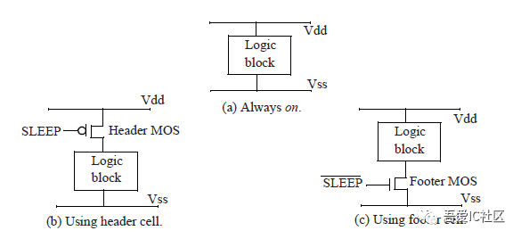
2. Power Gating. This strategy is often used in digital IC back-end design to reduce power consumption. During the back-end implementation process, MTCMOS is added to control the switching of standard cells.
3. Multi-Vt Cells. This involves using HVT or RVT in areas that are not part of the critical path during the digital IC back-end design process to reduce leakage. Of course, this requires a trade-off with performance and area, as using HVT or RVT may lead to timing issues, making optimization difficult, which could potentially increase the area instead of reducing it.
4. DVFS Technology. DVFS (Dynamic Voltage and Frequency Scaling) is essentially a low-power technology that adjusts the operating voltage and clock frequency based on the actual power consumption needs of the chip at that moment. This ensures that the provided power meets the requirements without excess, thus reducing power consumption. For example, in digital chips, the CPU module (such as an 8-core CPU) can be supplied with a higher voltage (overdrive) via software when it needs to perform at a higher frequency. In a particular application scenario, if the CPU only needs a lower frequency, the voltage can be adjusted to a lower voltage (underdrive) to achieve this.
Simply reducing frequency and voltage will not necessarily lower power consumption, as running at low frequencies may increase the time required for the system to process tasks, which could overall lead to increased power consumption. Therefore, the core of DVFS is the dynamic adjustment strategy, which aims to adjust in real-time based on the current system load, thus providing the minimum power that meets the current performance requirements and achieving the lowest power consumption. Before formulating the adjustment strategy, it is essential to identify the major power-consuming modules in the system, such as the CPU and GPU. The basic strategy is to increase frequency and voltage as the workload increases and decrease frequency and voltage as the workload decreases.
5. Well Bias. This method can dynamically adjust the bias voltage to achieve the goal of reducing power consumption.
That’s all for today’s writing. It’s not easy to create original content, so if you like it, please help share it. Thank you in advance! Meanwhile, the 52-IC Community (52-ic.com) has officially launched. The 52-IC Community is a professional platform for sharing and discussing digital IC design and implementation technologies and experiences. If you encounter technical problems in your studies or work, feel free to ask and discuss on our website.

[This article was published by “52-IC” on March 3, 2018]