Click the card below to follow Arm Technology Academy
This article is authorized to be reprinted from the WeChat public account TrustZone. This article mainly introduces how to reduce power consumption at various levels of chip design.
1 Introduction
In chip design, we often mention the PPA trade-off, which stands for Power, Performance, and Area.
The motivation for low-power design mainly includes the following aspects:
● Excessive power consumption can lead to a decrease in battery life for portable devices,
● Increased heat dissipation costs for chips,
● Higher temperatures can affect the reliability of chips and the timing of circuits,
● Increased difficulty in power grid design,
● And reduced competitiveness of products.
To alleviate the above issues, we will adopt corresponding PPA design techniques at various stages of system, architecture, front-end, back-end, production, process, and mass production.
2 Analysis of Power Consumption Sources
As we understand, power consumption is mainly divided into static power consumption and dynamic power consumption. Among them, dynamic power consumption accounts for about 80%.
2.1 Dynamic Power Consumption
Dynamic power consumption is the power consumed due to logic transitions when the output of gate circuits switches. It is divided into:
Dynamic power consumption = switching power + short-circuit power
Switching power refers to the power consumed during the charging and discharging of the load capacitance when the output of CMOS circuits flips. The load capacitance includes net capacitance and gate capacitance.
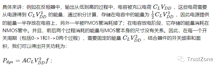
Where A is the circuit flipping activity factor; C is the circuit load charge and inherent capacitance; f is the operating frequency of the circuit; Vdd is the supply voltage.
2.2 Static Power Consumption
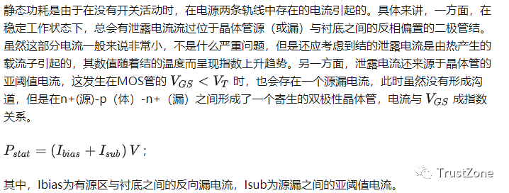
3 Technologies for Reducing Power Consumption
3.1 Reducing Power Consumption at Different Levels
Reducing power consumption should be carried out at multiple design levels, including: system level, logic level, and physical level. The higher the level, the greater the benefit.
3.2 Architectural Level Power Reduction
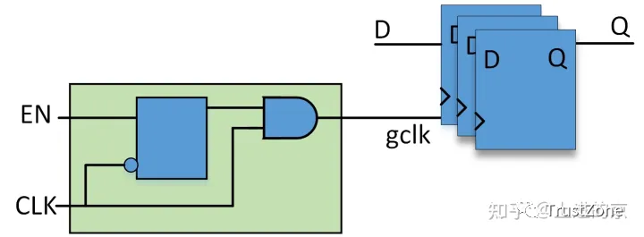
3.2.1 Clock Gating
In switching power, the majority is generated by clock distribution, therefore, most of the unused circuits can be turned off by clock gating, thereby reducing power consumption.
Clock gating technology is mainly divided into: combinational clock gating schemes and sequential clock gating schemes.
Among them, sequential gating adds a flip-flop, which is not suitable for multi-bit wide data, and relevant literature indicates that: sequential clock gating transitions are only more efficient in the case of more than 16 flip-flops.
3.2.2 Dynamic Voltage/Frequency Scaling (DVFS)
The dynamic technology adjusts the chip’s operating frequency and voltage dynamically according to the different computational needs of the application program running on the chip (for the same chip, the higher the frequency, the higher the required voltage), thus achieving the goal of reducing power consumption. The specific steps can be summarized as follows: first, collect system load-related signals, calculate the current system load; then predict the system’s performance requirements for the next time period based on the current load; calculate the frequency required for the system to operate; finally, calculate the corresponding voltage based on the new frequency and adjust the supply voltage.
3.2.3 Adaptive Voltage Scaling (AVS)
Adaptive Voltage Scaling provides different voltages for chips with different process corners, thus fully utilizing timing margins to reduce chip power consumption.
The advantage of AVS is that it can ensure that the system operates correctly at the lowest voltage required, compensating for the effects of process variations, clock frequency changes, and power converter offsets, while meeting system performance requirements, thus achieving power savings.
3.2.4 Power Gating
Power gating, also known as power cut-off technology, refers to adding switches to the chip to selectively cut off the supply current based on application requirements. On one hand, for fine-grained power gating, some switching transistors need to be added, thus requiring coordination with standard cell units. On the other hand, for coarse-grained power gating, the transistors are part of the power network rather than part of standard cells.
Benefits: Can eliminate the power consumption of the entire turned-off module;
Implementation: Can be controlled by board-level power control or by on-chip MTCOMS switch units.
3.2.5 Multi-Threshold Voltage (Multi-Vth)
Multi-threshold voltage technology refers to mixing multiple voltage threshold logic units in the same chip. A typical multi-supply library contains at least two sets of functionally identical but different threshold voltage units. Multi-Vdd will bring interconnect communication issues between different voltage domains, and special units called level shifters are required.
Principle: MOS transistors require a certain voltage to conduct; low-threshold voltage units require lower conduction voltages, so compared to high-threshold voltage units, they conduct faster, resulting in more leakage current and higher power consumption.
Recommendation: Use low-threshold units on timing-critical paths and high-threshold units on timing-relaxed paths.
Usage impact: Logic units with different thresholds have the same area/shape, so they can be replaced at various stages of the project without affecting the work of the front-end and back-end.
Usage method: The selection and replacement of different threshold logic units are automatically completed by the tools through setting instructions during synthesis and back-end processes, without special handling of front-end code. On one hand, if the ultimate design goal is to meet performance, low-threshold units can be used for the first synthesis to achieve the best performance to meet timing requirements, and then replace the parts that do not require high performance with high-threshold voltage units to reduce overall leakage current and power consumption. On the other hand, if the primary design goal is power consumption, it is more appropriate to use high-threshold voltage units during the first synthesis and then identify critical paths to replace them with low-threshold voltage units.
3.2.6 Multi-Voltage Supply (Multi-Vdd)
Since dynamic power consumption is proportional to the square of the supply voltage, reducing the voltage value will yield significant power savings; in addition, static power consumption is also proportional to the supply voltage, which will also have benefits.
Implementation method: Divide the design into independent “voltage leads” or “voltage domains” and use different supply voltages according to the timing requirements of each area. For example, modules with strict timing requirements operate at standard voltage (1V for 90nm process); paths with less strict timing requirements can be arranged in other low-voltage areas, such as 0.8V.
Additional considerations: Timing of cross-voltage domain paths may be affected, and timing margins need to be considered during design.
3.3 Reducing Power Consumption at Register Transfer Level
3.3.1 State Machine Encoding and Decoding
State machine encoding has a significant impact on signal activity. By reasonably selecting the encoding method for state machine states, power consumption can be reduced by minimizing circuit flips during state machine transitions. The main principles are as follows:
● For frequently switching adjacent states, try to use adjacent encoding state machine encoding, such as prioritizing Gray code (which can also eliminate the risk of glitches associated with state combination equations).
● Small state machines can choose one-hot code encoding, where only 1 bit needs to be concerned during state comparisons.
● Avoid redundant states in the state machine, and identify equivalent states.
3.3.2 Automatic Clock Gating Encoding
With a certain coding style, synthesis tools can automatically synthesize clock gating circuits from RTL, thus maximizing gating coverage.
Writing style:
● In always statements, write the last else as data_out<=data_out (or omit the else branch, as sequential logic inherently maintains state).
always @(posedge clk or negedge rst_n) begin if(!rst_n) data_out <= 32'b0; else if (enable) data_out <= data_in; //else // data_out <= data_out; end● The last branch cannot be written as data_out<=data_out, and is a level condition. Therefore, the last branch can be further divided into two branches: one branch is based on this valid level signal form of pulse signal condition; the other branch is the last else holding behavior. This writing style requires converting the level signal into a pulse condition, so a DFF needs to be added; thus, it is necessary to weigh whether this modification is cost-effective.
For example:
always @(posedge clk or negedge rst_n) begin if(!rst_n) data_out <= 32'd0; else if (enable) data_out <= data_in; else data_out <= 32'd0; end Change it to:
always @(posedge clk or negedge rst_n) begin if(!rst_n) data_out <= 32'd0; else if (enable == 1'b1) data_out <= data_in; else if (enable_negedge_pulse == 1'b1) data_out <= 32'd0; end //enable_negedge_pulse signal is the falling edge pulse of the enable signal assign enable_negedge_pulse = ~enable & enable_dly; always @(posedge clk or negedge rst_n) begin if(!rst_n) enable_dly <= 1'b0; else enable_dly <= enable; end3.3.3 One-Hot Code Multiplexer
For the generation of multiplexers, “case” statements, “if” statements, and state machines can all be used. However, using binary encoding can lead to frequent data flips entering cascading muxes, resulting in noticeable switching processes and increased power consumption. If one-hot encoding is used, outputs will be faster and more stable, and frequent data flips will be suppressed by the select signal, hiding unselected lines, thus achieving low power consumption.
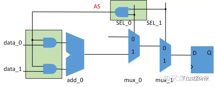
3.3.4 Operand Isolation Technique
During arithmetic operations, keep the module’s inputs open for effective logical operations; when not performing operations, keep the module’s inputs unchanged to avoid unnecessary flips.
As shown in the figure, the signal AS=SEL_0&!SEL_1 serves as the operand isolation signal, allowing operands data_0 and data_1 to enter add_0 only when AS is 1; when AS=0, add_0 does not operate, and the output structure does not flip.
4 References
[1] “Digital Integrated Circuits – Circuits, Systems, and Design”
[2] “The Art of Hardware Architecture”
[3] Zhiyuan Class Course Content
Recommended Reading
-
Detailed Explanation of SoC Chip Design Verification
-
Chip Creation | Interview with Ling Si Technology: Deep Coupling of SoC Chips + AI Algorithms Driving Intelligent Connectivity
-
What is the Difference Between Heterogeneous Processors HPU and System-on-Chip SoC?


Long press to recognize the QR code to add Miss Jishu’s WeChat (aijishu20) and join the Arm Power Consumption Group.
Follow Arm Technology Academy
 Click the “Read Original” button below to see more articles about IC design.