
“Automotive Controller Disassembly” column will share disassembly analysis of intelligent automotive controllers, presenting the latest mass-produced controller reference designs and selection schemes to readers.
This article will decode the design scheme of SAIC Roewe RX5 MAX domain controller. The Tier1 of this scheme is the joint venture company of SAIC and TTTech, Chuangshi Intelligent Driving. The Roewe RX5 MAX is equipped with 3 millimeter-wave radars, 6 full HD cameras, and 12 ultrasonic radars, enabling approximately 20 intelligent assisted driving functions.
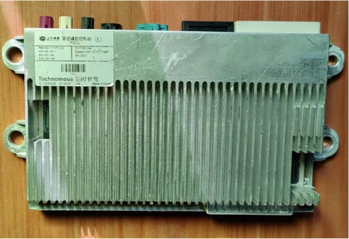
Front View of the Autonomous Driving Domain Controller Enclosure
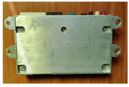
Back View of the Autonomous Driving Domain Controller Enclosure
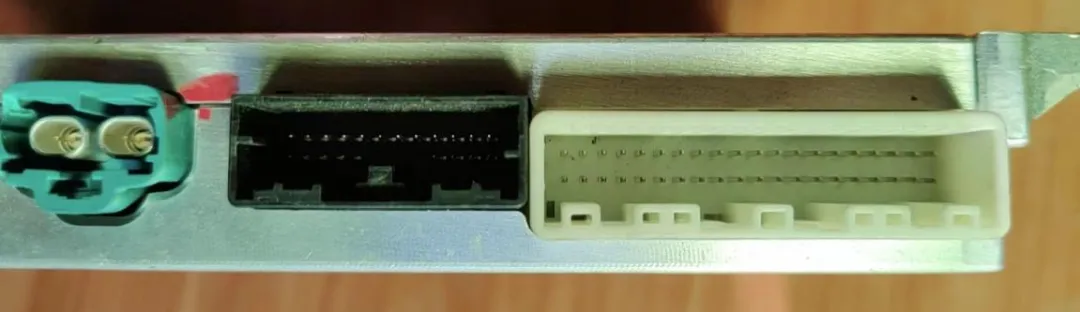
The above image shows the power, CAN, GPIO, and gigabit Ethernet terminal interface diagram of Chuangshi Intelligent Driving domain controller
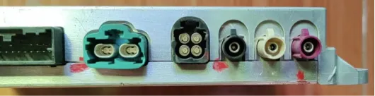
The above image shows the camera and antenna terminal diagram of Chuangshi Intelligent Driving
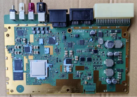
Front View of PCB
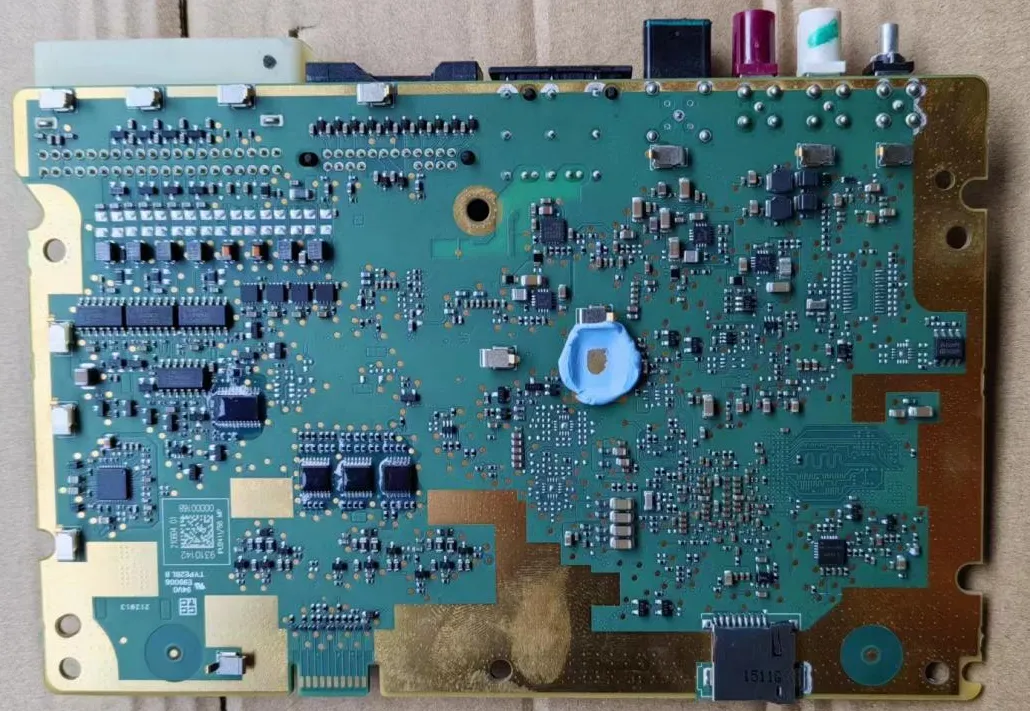
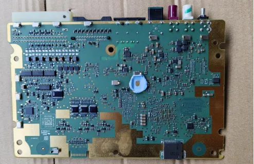
Back View of PCB
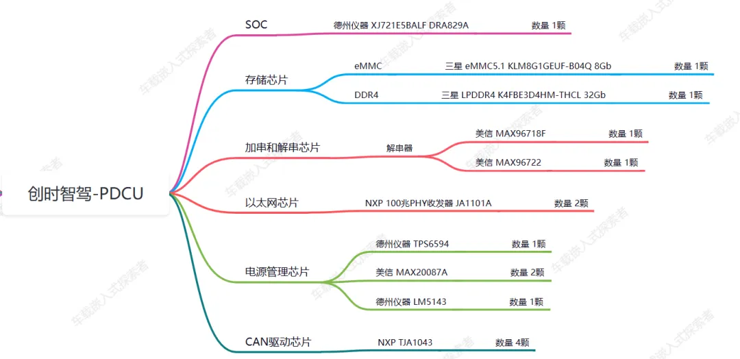
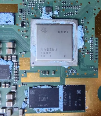
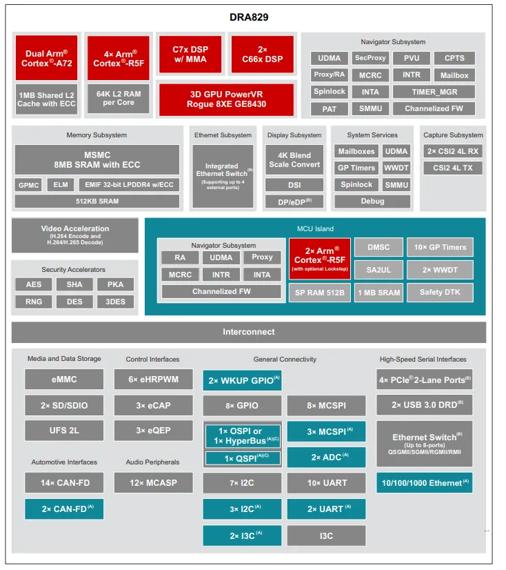
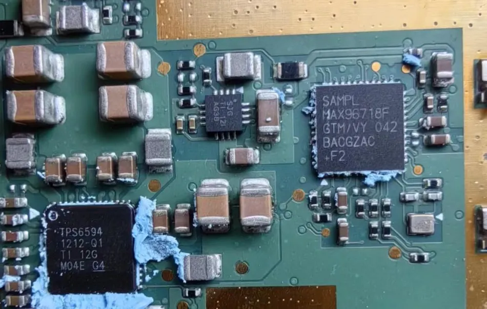
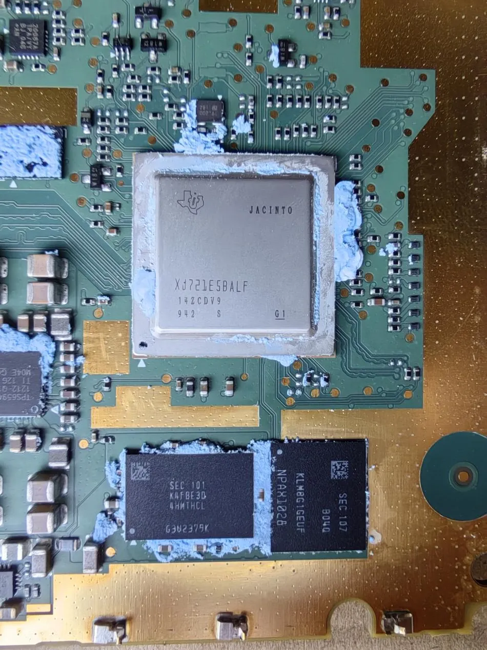
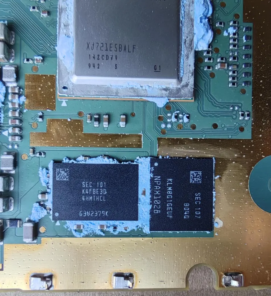
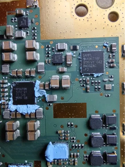
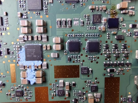
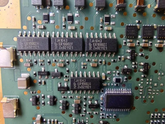
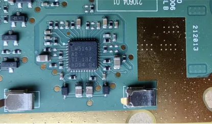
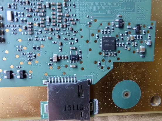
Chuangshi Intelligent Driving’s domain controller uses a Texas Instruments DRA829 as the main control SOC, responsible for carrying out algorithms for perception, planning, etc.; the storage chip consists of a Samsung EMMC chip and a DDR4 chip; the deserializer uses a Maxim MAX96718 and MAX96722; the Ethernet chip is NXP’s JA1101A; the power management chip is a Texas Instruments TPS6594, two Maxim MAX20087, and a Texas Instruments LM5143; the CAN bus driver chip is NXP’s TJA1043. The following will explain the characteristics and functions of each chip in detail..
4.1, SOC Chip
4.1.1, Introduction to DRA829
The DRV829 processor is based on the evolving Jacinto™ 7 architecture, aimed at ADAS and autonomous vehicle (AV) applications, built on TI’s extensive market knowledge accumulated over more than a decade in the ADAS processor market. In an architecture aimed at meeting functional safety standards, the unique combination of high-performance computing, deep learning engines, and dedicated accelerators for signal and image processing makes the DRA829 device highly suitable for various industrial applications such as robotics, machine vision, radar, etc. The DRA829 provides high-performance computing for traditional and deep learning algorithms with an industry-leading power/performance ratio, and has a high degree of system integration, enabling scalability and lower cost for advanced automotive platforms that support multiple sensor modes in centralized ECUs or standalone sensors. Key cores include next-generation DSPs with scalar and vector cores, dedicated deep learning and traditional algorithm accelerators, the latest Arm and GPU processors for general computing, integrated next-generation imaging subsystems (ISP), video codecs, Ethernet hubs, and isolated MCU islands, all protected by automotive-grade safety hardware accelerators.
4.1.2, Role of DRA829 in Domain Controller
①, Perception Processing: The DRA829 achieves real-time processing and fusion of multi-sensor data for target detection, target recognition, lane departure warning, pedestrian recognition, and other functions through integrated high-performance processors and digital signal processors (DSPs). It can process data from various sensors such as cameras, millimeter-wave radars, ultrasonic sensors, etc.
②, Data Transmission and Storage: The DRA829 has high-speed data transmission and storage capabilities, supporting multi-channel high-speed data interfaces such as Ethernet, USB, CAN, etc., for real-time reception and transmission of sensor data. In addition, TDA4 also supports high-capacity storage devices that can store large amounts of onboard data for offline analysis and post-processing.
③, Decision Making and Planning: The DRA829 is equipped with a high-performance AI processor that can perform real-time decision-making and planning. It can predict and analyze the environment through deep learning models, generating safe and efficient path planning and dynamic decision-making for the navigation and driving control of autonomous vehicles.
④, Safety Assurance: The DRA829 has multiple safety mechanisms, including hardware encryption, cellular communication security, and system integrity checks. It can ensure the secure transmission and storage of sensitive data, enhancing the safety performance of the autonomous driving system.
4.1.3, Features
|
|
|
|
|
|
|
|
|
|
|
|
|
|
|
|
|
|
|
|
|
|
|
|
Block Diagram
4.2, Storage Chips
4.2.1, LDDR4-K4FBE3D4HM
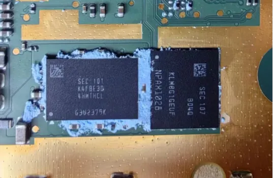
K4FBE3D4HM Introduction
Storage capacity: 32GB
Read/write speed: 4266 Mbps
Function:
①, LPDDR4 can provide fast storage access speeds and high bandwidth, which is necessary for autonomous driving systems to perceive and analyze environmental data around the vehicle in real-time, including images, radar data, etc. The high-speed read and write capabilities of LPDDR4 can accelerate data transmission speed between the storage and processor, thereby improving the system’s response speed and real-time performance.
②, LPDDR4 features low power consumption. Autonomous driving systems require stable operation for extended periods and typically operate in embedded environments, where heat dissipation and power consumption control are essential considerations. The low power design of LPDDR4 can reduce the energy consumption of the controller, extend battery life, and minimize heat dissipation issues, enhancing system stability and reliability.
③, LPDDR4 supports high-density storage and large-capacity memory, which is needed for autonomous driving systems to store and manage large amounts of map data, vehicle status data, historical control information, etc. The high-density storage capabilities of LPDDR4 can meet these needs while ensuring high-speed read and write performance.
Features
|
• Double data rate architecture; two data transfers per clock cycle • Bidirectional data strobe (DQS_t, DQS_c) sent/received with data used by the receiver when capturing data • Differential clock input (CK_t and CK_c) • Differential data strobe (DQS_t and DQS_c) • Command and address inputs on the positive CK edge; two edges of DQS reference data and data mask • Each mold consists of 2 channels • Each channel has 8 internal banks • DMI pin: normal write and read operation’s DBI (data bus inversion), DMI off is used for masking write data (DM) -DBI on masks write DQ 1’s count# • Burst length: 16, 32 (OTF) • Burst type: continuous • Read/write latency: see Table 64 LPDDR4 AC timing table • Auto-precharge option for each burst access • Configurable drive strength • Refresh and self-refresh modes • Partial array self-refresh and temperature-compensated self-refresh • Write leveling • CA calibration • Internal VREF and VREF training • FIFO-based write/read training • MPC (multi-purpose command) • LVSTL (low-voltage swing terminated logic) IO • VDD1/VDD2/VDDQ:1.8V/1.1V/1.1V • VSSQ terminal • No DLL: CK to DQS not synchronized • Edge-aligned data output, data input center-aligned write training • Refresh rate: 3.9us |
4.2.2, eMMC KLM8G1GETF
KLM8G1GETF-B041 Introduction
Storage capacity: 64GB
Function:
①, This EMMC chip is one of the main media for storing firmware and operating systems of the controller. The firmware and operating systems of the main controller are burned into the EMMC chip to load from the chip at startup. This ensures system stability and consistency, enabling the controller to start quickly.
②, The EMMC chip is also responsible for storing and managing the operational code in the controller. Autonomous driving controllers need to process a large amount of data and complex algorithms, and the running programs have very high requirements for real-time performance. The EMMC chip provides fast data read and write speeds, effectively executing the operational code of the controller and ensuring its normal operation.
③, The EMMC chip is also used to store and manage data within the controller. Autonomous driving systems need to record and store various sensor data, map data, and other important information in real-time to support real-time decision-making and improve algorithms. The EMMC chip provides large-capacity storage space and high-speed data read and write capabilities, meeting the data storage requirements of autonomous driving controllers.
4.3, Serializer/Deserializer Chips
4.3.1, Maxim MAX96722
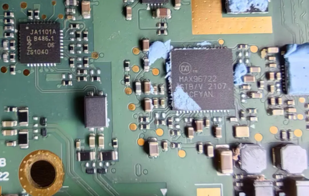
Introduction
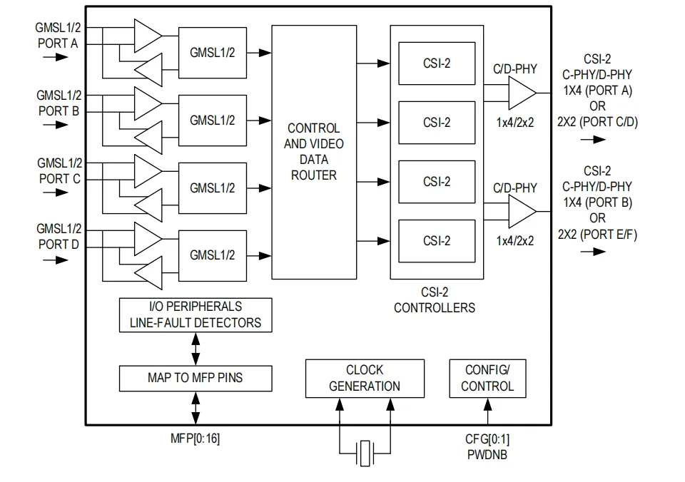
The MAX96722 deserializer converts GMSL2 or GMSL1 serial inputs into MIPI CSI-2 D-PHY or C-PHY format outputs. This device allows simultaneous transmission of bidirectional control channel data while performing forward video transmission on each link. The MAX96722 can accommodate up to four remote sensors using industry-standard coaxial cables or STP interconnects. Each GMSL2 serial link operates at a fixed rate of 3Gbps in the forward direction and 187.5Mbps in the reverse direction. In GMSL1 mode, the MAX96722 can pair with first-generation 3.12Gbps or 1.5Gbps GMSL1 serializers, or operate with GMSL2 serializers in GMSL1 mode at up to 3.12Gbps.
MAX96722 supports the aggregation and replication of video data, allowing streams from multiple remote sensors to be combined and routed to one or more available CSI-2 outputs. Data can also be routed based on virtual channel IDs, allowing multiple streams from a single GMSL input to be routed independently to different CSI-2 outputs. Alternatively, frame-level cascading can be used to synchronize and combine data from multiple sensors into a single CSI-2 stream within a composite superframe. The CSI-2 interface supports 2×4 lane and 4×2 lane configurations using C-PHY or D-PHY.
Features
|
MIPI CSI-2 v1.3 output configurable as 2×4 lanes, 1×4 lane + 2×2 lanes, or 4×2 lanes |
|
|
Independently configurable four GMSL inputs GMSL1/2 operation, link speeds, and video formats |
|
|
Compatible with ASIL-B (GMSL2) |
|
|
|
|
|
|
|
|
|
|
|
|
4.3.2, Maxim MAX96718
Performance similar to MAX96722, detailed chip manual not found!
4.4, Ethernet/Switch Chip
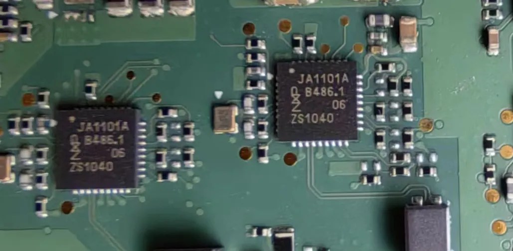
TJA1101 Introduction
The TJA1101 is an Ethernet PHY compliant with the 100BASE-T1 standard, optimized for automotive use cases such as gateways, IP camera links, driver assistance systems, and backbone networks. This device provides 100Mbit/s transmission and reception capability over two unshielded twisted pairs, supporting cable lengths of at least 15m.
The TJA1101 is designed for automotive robustness and ISO 26262, ASIL A compliance while minimizing power consumption and system costs. Due to its compliance with ASIL-A standards, sufficient safety features have been implemented to ensure that ASIL requirements are met at the system level.
Features
|
|
|
|
|
|
|
Optimized for automotive use cases |
|
|
|
|
|
|
|
|
|
|
Block Diagram
4.5, Power Management Chips
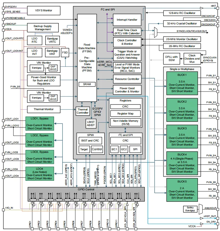
4.5.1, TPS6594
The TPS6594-Q1 features five buck converters and four LDOs, suitable for automotive safety-related applications.
Features
|
|
|
|
|
|
|
Complies with functional safety standards
|
|
|
|
|
|
Five switch-mode power buck regulators:
|
|
|
|
|
|
|
|
|
|
|
|
|
Functional Block Diagram

4.5.2, MAX20087
MAX20087 Introduction
Dual/Quad channel camera power protector; the industry’s only ASIL-rated camera protector, providing diagnostics via I2C. Maxim offers four camera power diagnostic chips: MAX20086, MAX20087, MAX20088, MAX20089.
MAX20086–MAX20089 dual/quad camera power detection ICs provide up to 600mA load current for each of the four output channels. Each output is individually protected against battery short circuits, ground short circuits, and over-current situations. The IC operates on a 3V to 5.5V supply and a 3V to 15V camera supply. At 300mA, the voltage drop from input to output is only 110mV (typical).
The IC provides enable inputs and an I2C interface to read the diagnostic status of the device. An onboard ADC can read the current through each switch. Versions compliant with ASIL B and ASIL D support reading an additional seven diagnostic measurements via the ADC, ensuring high fault coverage.
MAX20086–MAX20089 include over-temperature shutdown and over-current limit on each output channel. All devices are designed for ambient operating temperatures of -40°C to +125°C.
Features
|
|
|
|
Small solution size
|
|
|
|
|
|
|
|
|
|
4.5.2, MAX20087
|
Chip |
Price |
|
DRA829 |
700 |
|
Samsung eMMC5.1 KLM8G1GEUF |
18 |
|
Samsung LPDDR4 K4FBE3D4HM |
100 |
|
Maxim MAX96718F |
100 |
|
Maxim MAX96722 |
110 |
|
NXP 100M PHY transceiver JA1101A |
18*2 |
|
Texas Instruments TPS6594 |
80 |
|
Maxim MAX20087A |
20*2 |
|
NXP TJA1043 |
15*4 |
|
Texas Instruments LM5143 |
50 |
This column will continue to disassemble the latest controller schemes from both domestic and foreign sources, including but not limited to intelligent driving, cockpit, central computing, body domain control, chassis domain control, and power domain control.
To continuously launch popular controller disassemblies, this column will adopt a
crowdfunding
approach to purchase related domain controller samples. Friends participating in crowdfunding can place orders for controllers they are interested in and receive more detailed disassembly reports.
If you are willing to participate in crowdfunding disassembly, please contact the editor: btigh
teast.