Abstract
This article will introduce the disassembly analysis of smart vehicle controllers, presenting the latest reference designs and selection schemes for mass-produced controllers. Today, we will share the intelligent domain controller module T-BOX of SAIC Feifan R7.
The electronic architecture of SAIC Feifan R7 is developed by Zero束, consisting of four domain controllers: intelligent connectivity, intelligent computing, intelligent driving, and cockpit. The intelligent domain controller is similar to the traditional T-box module.
1. Introduction to T-BOX
2. Shell and Terminals
As shown in the figure, the TBOX shell consists of two metal parts, with the front metal shell designed with heat dissipation grooves.

Figure 1 TBOX Front

Figure 2 TBOX Back
2.2. Wiring Terminal Description:
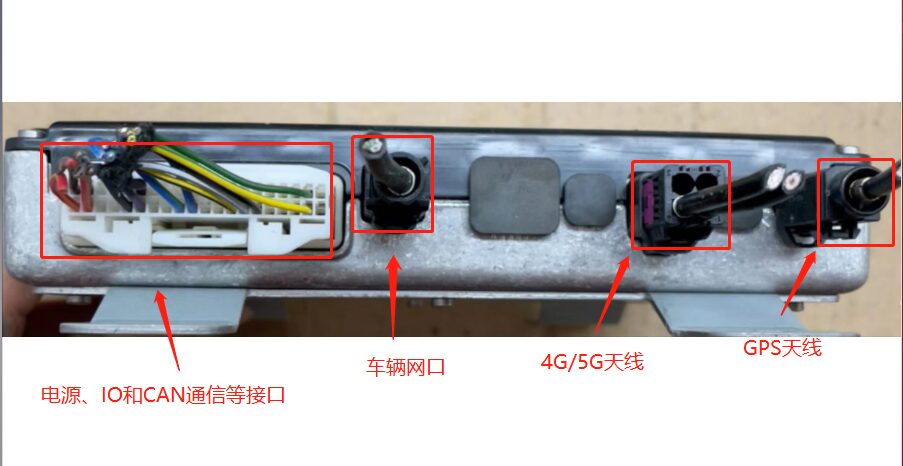
Figure 3 TBOX Wiring Terminals
The TBOX has terminals for power, UART/CAN bus, Ethernet port, 4G/5G antenna, and GPS antenna.
3. Composition of TBOX
The TBOX mainly consists of SOC chips, MCU chips, communication modules, encryption chips, switch chips, storage chips, power management chips, and GNSS modules. As shown in the figure:

Figure 4 Mind Map of Feifan R7 TBOX Composition
Functions of each module and commonly used schemes:
3.1. Role of SOC Chip and Common Models
The SOC chip is an important component in the automotive TBOX, responsible for processing vehicle information and realizing various functions. SOC chips usually consist of multiple cores, with each core responsible for different tasks, enabling the TBOX to perform multiple tasks simultaneously. Commonly used SOC chip models include NXP’s IMX6 and IMX8. These chips have powerful computing and image processing capabilities, supporting the playback of high-definition video and real-time image analysis, providing strong computing and processing power for the TBOX.
3.2. Role of MCU Chip and Common Models
The MCU chip is an important component for controlling various sensors and actuators in the vehicle, responsible for real-time monitoring of vehicle status and controlling the operation of various systems as needed. Commonly used MCU chip models include Infineon’s TC2x and TC3x series, NXP’s S32K14X, and Renesas R7F7X, etc. These chips feature high performance and low power consumption, meeting the needs of TBOX in vehicle control and monitoring.
3.3. Function of Communication Module and Common Module Models
The communication module is a key component in the TBOX that enables communication between the vehicle and the outside world. It can connect to the internet via wireless networks, facilitating the transmission of vehicle information and remote control. Common communication module models include Huawei’s ME909s, MH5000 series, and Quectel AG35, AG550, AG520, etc. These modules support 5G, 4G, and 3G networks, with Quectel AG520, AG550, and Huawei’s MH5000 supporting V2X, providing stable and reliable connectivity for high-speed data transmission and remote control functions.
3.4. Function of GPS Module and Common Module Models
The GPS module is a key component in the TBOX used for positioning and navigation. It can receive satellite signals and calculate the vehicle’s accurate position through positioning algorithms. Common GPS module models include: HeXin Star’s UM960, UM982 and ublox’s ZED-F9K, ZED-F9P, ZED-F9H, etc. These modules feature fast positioning, high precision, and stability, meeting the TBOX’s needs in navigation and positioning.
3.5. Function of Switch Chip and Common Chip Models
The switch chip is an important component in the TBOX that enables data exchange and communication, facilitating data transmission and interaction between various subsystems in the vehicle. Common switch chip models include Broadcom’s BCM89x series and MARVELL 88Q5050 series. These chips feature high bandwidth and low latency, enabling fast data transmission and real-time system interaction.
3.6. Function of Encryption Chip and Common Chip Models
The encryption chip is a key component in the TBOX that ensures data security and prevents malicious attacks. It can encrypt and decrypt data and implement access control and identity authentication functions. Common encryption chip models include Infineon’s SLE 95250 SLS32 series, Maxim’s DS28E25 series, and Shanghai Xintai’s TTM2000, TTM3000 series. These chips feature advanced encryption algorithms and security performance, protecting the data in the TBOX from unauthorized access and tampering.
4. Analysis of Feifan R7 TBOX
Feifan R7 TBOX Composition Block Diagram:

Figure 5 Composition Diagram of Feifan R7 TBOX
 Figure 6 PCB Front View

Figure 7 PCB Back View

Figure 8 PCB Side View
4.1. SOC – NXP MIMX8QX6AVLFZAC

Figure 9 MIMX8QX6AVLFZAC Physical Picture
NXP MIMX8QX6AVLFZAC Introduction
The i.MX 8X series processors are based on highly integrated architecture, supporting graphics, video, image processing, and voice functions, meeting the needs for security certification and high energy efficiency. Suitable applications include industrial automation and control, HMI, robotics, building control, automotive dashboards, video/audio, in-vehicle infotainment systems, and in-vehicle information services, etc.

Figure 10 i.MX 8X Block Diagram
Features:
|
Processor Composite Device |
·2-4 Cortex-A35 cores ·1 Cortex-M4F core for real-time processing ·1 Tensilica® HiFi 4 DSP |
|
Multimedia |
·2-4 Vec4-Shader GPUs, OpenGL® ES 3.1, OpenCL™ 1.2 EP, OpenVG™ 1.1, Vulkan® ·Video: 4K H.265 dec | 1080p H.264 enc / dec |
|
Memory |
·16/32-bit DDR3L-1866 and LPDDR4-2400 ·1 Octal SPI or 2 Quad SPI ·ECC function ①.Cortex-A35 L1 cache parity ②.Cortex-A35 L2 cache ECC ③.ECC protection on sDDR interface |
|
Display & Camera |
·2 Combined MIPI DSI (4 channels) / LVDS (1080p) ·24-bit Parallel Display I/F (WXGA) ·SafeAssure® fault recovery display ·1 4-channel MIPI CSI2 ·1 Parallel 8-bit CSI (BT.656) |
|
Connectivity |
·2 SDIO3.0 [or 1 SDIO3.0 + 1 eMMC5.1] ·USB 2.0 and 3.0 OTG support, with PHY ·2 Ethernet AVB MACs ·3 CAN / CAN FD ·MOST 25/50 ·PCIe 3.0 (single channel), provides L1 sub-state ·1 12-bit ADC (6 channels) ·4 SPIs, 1 ESAI, 4 SAIs, 1 keyboard ·4 I2Cs (high-speed), 4 I2Cs (low-speed) ·1 SPDIF |
|
Safety |
·High reliability boot, SHE ·TRNG, AES-128, AES-256, 3DES, ARC4, RSA4096, SHA-1, SHA-2, SHA-256, MD-5 ·RSA-1024, 2048, 3072, 4096 and secure key storage ·10 tamper pins (active and passive) ·Online encryption engine (AES-128) |
4.2. MCU – Renesas R7F7015833

Figure 11 R7F7015833 Physical Picture
R7F7015833 is Renesas’s automotive-grade chip RH850. RH850 Product Combination Diagram:

RH850 Introduction:
RH850/C1M-Ax microcontroller is equipped with RH850 series G3MH (C1M-A2 is dual-core) CPU core (C1M-A1 operating frequency is 240MHz, C1M-A2 operating frequency is 320MHz), with excellent processing capabilities. In addition to ROM, RAM, and DMA, this microcontroller also integrates various timers (such as motor control timers), various serial interfaces (such as CAN, which is CAN FD compatible), 12-bit A/D converters (ADC), R/D converters (RDC3A) that convert rotary transformer output signals into digital angle information, CPUs, and parallel motor control units (EMU3), etc., equipped with various peripheral functions suitable for HEV/EV motor control. In addition, C1M-A2 can simultaneously control two motors.

RH850 Features:
|
CPU Core: |
C1M-A1: 240MHz Core (includes lock-step dual-core x1) C1M-A2: 320MHz Core x2 (includes lock-step dual-core x1) FPU |
|
Timer: |
Main oscillator: 20MHz PLL with optional SSCG mode: 240MHz or 320MHz PLL without SSCG mode: 80MHz On-chip low-speed oscillator: 240kHz Data transfer: DMAC / DTS |
|
Timers: |
Timer Array Unit D (TAUD) 2 or 4 units Timer Array Unit J (TAUJ) 1 or 2 units Motor Control Timer (TSG3) 2 or 3 units Encoder Timer (ENCA) 2 units |
|
Analog: |
SAR A/D converter 30 or 48 channels, 3 units |
|
Communication Interface: |
Clock Serial Interface H (CSIH) 3 channels CAN Interface (RS-CANFD) 4 channels LIN Interface (RLIN3) 3 channels Serial Communication Interface (SCI3) 3 channels RSENT 4 channels |
|
Motor Control: |
Motor Control Timer (TSG3) 2 or 3 units R/D Converter (RDC3A) 1 or 2 units Enhanced Motor Control Unit (EMU3) 1 unit |
|
Safety: |
Multi-input signature generator (MIST) Clock monitor Watchdog timer Safety watchdog timer Memory protection function |
|
Power Voltage: |
1.15V – 1.35V (CPU core) 4.5V – 5.5V (I/O, system, AD converter, RD converter) |
|
Temperature: |
Tj= -40° – +150° |
4.3. 5G+V2X Module – Quectel AG550

AG550 Introduction:
AG55xQ is a series of automotive-grade 5G NR Sub-6 GHz modules developed by Quectel, supporting both standalone (SA) and non-standalone (NSA) modes of 5G NR networking. Utilizing 3GPP Rel-15 technology, the module can support a maximum downlink rate of 2.4 Gbps and an uplink rate of 550 Mbps under 5G NSA mode, and a maximum downlink rate of 1.6 Gbps and an uplink rate of 200 Mbps under LTE-A networks. Through its C-V2X PC5 direct communication function (optional), AG55xQ can be widely applied in the field of Internet of Vehicles, providing reliable solutions for the establishment of smart cars, autonomous driving, and intelligent transportation systems. Additionally, the module supports dual SIM dual standby (optional) and rich functional interfaces, greatly facilitating application development for customers. Its excellent ESD and EMI protection performance ensures strong robustness in harsh environments.
AG55xQ includes AG550Q (5G + DSSS + C-V2X), AG551Q (5G + DSSS), AG552Q (5G + DSDA), and AG553Q (5G + DSDA + C-V2X); to meet different market needs, each series includes multiple models: AG55xQ-CN, AG55xQ-EU, AG55xQ-NA, and AG55xQ-JP. At the same time, each series of modules is backward compatible with existing GSM, UMTS, and LTE networks, allowing connectivity in areas without deployed 5G NR networks and remote areas without 3G/4G network coverage.
AG550 Features:
·Complies with IATF 16949 and APQP, PPAP automotive industry quality management process requirements based on Qualcomm SA515M chip (AEC-Q100 standard compliant) developed automotive-grade solutions
·5G NR Sub-6 GHz module, supporting both standalone and non-standalone networking modes
·Backward compatible with 4G (Cat 19)/3G/2G networks
·MIMO technology meets the requirements of wireless communication systems for data rates and connection reliability
·Optional C-V2X PC5 Mode 4 direct communication
·Optional dual SIM dual standby technology (DSDA), meeting different application needs of customers
·Optional single-frequency GNSS, dual-frequency GNSS, PPE (RTK), and GNSS/QDR combined navigation solutions, meeting varying degrees of positioning accuracy and speed requirements in different environments
·Enhanced functional features: DFOTA, VoLTE, QuecOpen®, high security, etc.
·Ultra-wide operating temperature range (-40 °C ~ +85 °C), eCall applications below +95 °C, superior electromagnetic interference resistance to meet the application needs of automotive and other harsh environments
4.4. Encryption Chip – Xintai TTM2000A11

Xintai TTM2000A11 Introduction:
Mizar TTM2000 is a flexible, reliable, secure, and compliant encryption chip product designed for the automotive electronics field. This product is specifically developed for the security of Internet of Vehicles V2X applications, fully meeting the message authentication performance, security certificate management, and other requirements needed for applications such as C-V2X and DSRC.
TTM2000 Features:
|
Standards and Certifications |
– EVITA hardware security module Full-level architecture design – AEC-Q100 Grade 1 requirements – National Cryptography Bureau security chip Grade 2 |
|
Product Features |
– ARM® SecureCore® SC300™ 32-Bit RISC Core, 80Mhz – 120.0DMIPS (Dhrystone v2.1); – Memory Protection Unit (MPU); – 24-bit SysTick timer; – 3.3V and 1.8V power supply, IO pin level is 3.3V – Operating temperature range: -40℃ – 125℃ – Package LQFP-64, QFN-64 (TBD) |
|
Security Features |
– Hardware “root of trust” anti-tampering detection function, physical shielding layer protection design, side-channel attack protection design – Internal integration of international standards and China National Cryptography Bureau standards hardware cryptographic algorithm units – 4 independent TRNGs – Hardware encrypted Flash, key encrypted secure storage – Watchdog timer (WDT) – High/low voltage anomaly detection – Temperature anomaly detection |
|
Cryptographic Algorithm Unit |
– High-speed ECDSA (NIST-P256) – High-speed SM2 – High-speed SM3 – RSA (up to 2048 bits) – ECC-256 – SHA-256 – AES – DES – SM4 |
|
System Protection |
– Each chip has a unique 32-bit serial number – Comprehensive lifecycle state management – System secure boot using domestic cryptographic algorithms |
|
Communication Features |
– 2 integrated SPI controllers, configurable as Master/Slave mode – 1 UART controller – 1 I2C – 5-channel GPIO, configurable as Input/Output, or as external interrupt input; – 1 external timer – 1 Watchdog – 8-channel DMA controller – Various types, configurable IO connections for better performance and flexibility |
|
Memory |
– 512KB internal Flash, ECC supported – 160KB SRAM – Secure ROM |
|
Key Cryptographic Unit Performance Design Goals |
– Ultra-high-speed SM2/ECDSA (NIST P-256) unit: >4000 signature verifications/second; – High-speed general curvature ECDSA unit: >1500 signature verifications/second; – High-speed SM3 unit: >500Mbps – High-speed SHA unit: >500Mbps |
4.5. Switch Chip – MARVELL 88Q5050

Marvell 88Q5050 Introduction:
Marvell 88Q5050 is an 8-port, high-security automotive Gigabit Ethernet switch chip that fully complies with IEEE802.3 and 802.1 automotive standards, featuring advanced security functions to prevent network threats (such as hacking and denial of service (DoS) attacks). This 8-port Ethernet switch chip has 4 fixed IEEE 100BASE-T1 ports and 4 configurable ports, which can include 1 IEEE 100BASE-T1, 1 IEEE 100BASE-TX, 2 MII/RMII/RGMII, 1 GMII port, and 1 SGMII port. The switch chip provides local and remote management functions, allowing users to easily access and configure the device. Through AEC-Q100 Level 2 certification, this solution employs Marvell’s highest hardware security features designed for automotive Ethernet chip security roots to prevent malicious attacks or threats to data streams within the vehicle. This advanced switch chip utilizes deep packet inspection (DPI) technology and secure boot functions to provide the industry’s most secure automotive Ethernet switch. All Ethernet ports support address blacklisting and whitelisting functions to further enhance security.
Block Diagram

Features
|
Processor |
Integrated ARM Cortex-M7 CPU, 250 MHz |
|
IO Interface |
•4 IEEE 100BASE-T1 •The remaining four ports can be configured as follows: – IEEE 100BASE-T1 – IEEE 100BASE-TX – MII/RMII/RGMII – GMII – SGMII •2 SMI – The main interface can connect to external PHY or other switches – The subordinate interface is used for managing the switch •Configurable GPIO •Working clock frequency configurable (19.2 MHz-83.3 MHz) QSPI interface •TWSI master interface •JTAG |
|
Package Features |
128-pin LQFP package, 0.5 mm pitch, 14 mm x 20 mm |
|
EEPROM |
Subordinate interface with loader for configuring the switch (32 Kb-512 Kb) |
|
Switch Matrix |
Gigabit switch matrix |
4.6. Storage Chip
eMMC Samsung 8G KLM8G1GEUF
DDR4 Samsung 2G K4F6E3S4HM

①、KLM8G1GEUF
Samsung eMMC is designed in BGA package form as an embedded MMC solution. eMMC operates the same as MMC devices, making it easy to read and write memory using the MMC protocol v5.1 (industry standard).
eMMC consists of NAND flash memory and an MMC controller. The NAND area (VDDF or VCC) requires a 3V power supply voltage, while the 1.8V or 3V dual power supply MMC controller supports voltage (VDD or VCCQ). Samsung eMMC supports HS400 to improve sequential bandwidth, especially sequential read performance.
Using eMMC has several advantages. It is easy to use, as the MMC interface allows easy integration with any microprocessor with an MMC host.
Since the embedded MMC controller isolates NAND technology from the host, any revisions or corrections to NAND are invisible to the host. This leads to faster product development and shorter time to market.

②、DDR4 Samsung 2G K4F6E3S4HM
K4F6E3S4HM-THCL is a multifunctional LPDRAM, ideal for mobile solutions. Samsung’s LPDDR4 is a breakthrough product that not only offers faster data transfer speeds but also lower power consumption, providing more design options for ultra-thin devices, artificial intelligence (AI), virtual reality (VR), and wearable devices.
Features:
•Refresh rate: 3.9us
4.7. GNSS Module – UBLOX ZED-F9K-00B

ZED-F9K Introduction
The ZED-F9K module uses the u-blox F9 GNSS platform to provide continuous decimeter-level positioning accuracy for the most challenging automotive use cases. LAP 1.30 supports L1/L2/E5B and L1/L5 frequency bands for maximum flexibility, satellite availability, and security. Complex built-in algorithms cleverly fuse IMU data, GNSS measurements, wheel ticks, and vehicle dynamics models to identify individual GNSS lane failures. The module natively supports u-blox PointPerfect GNSS enhancement services. It offers various global navigation satellite systems and IMU outputs in parallel to support all possible architectures, including a 50 Hz sensor fuse solution with very low latency. It also enables advanced real-time applications such as augmented reality while maximizing the number of visible satellites, even in urban conditions. This device is a standalone solution that provides the best possible system performance.
END
Click the business card below
Follow us now